Improving Extreme Temp Performance in EV Batteries

Submitted by Staff on

The limiting factors in automotive electrification today are the speed to charge the battery and the energy conversion efficiency to usable work, such as the EV range or thermal management of the passenger cabin. Extreme temperatures significantly negatively affect the vehicle's performance and battery durability. Energy harvesting can help the battery thermal management systems (BTMS) regulate the battery temperature in extreme ambients to optimize performance and range, increase the charging speed, or control the cabin temperature. For EVs to become truly mainstream, they must provide the performance drivers expect in all conditions, including extreme heat (100°F and above) and cold (20°F and below).

What is Energy Harvesting in EVs?

Energy harvesting, often called energy recovery in automotive applications, captures ambient energy, and converts it to electrical energy. This concept applies to all available ambient energy sources, including solar, wind, vibration, or thermal radiation. It can power ultra-low power MCUs to reduce small-load battery demand or MEMS sensors that monitor vehicle performance items.

For the larger-scale challenge of electric vehicles, the additional recovered energy augments the vehicle's primary energy load during operation, increasing its efficiency, and extending the range. Another benefit occurs during charging, where recovered waste energy from charging can warm the battery or preheat the cabin during extreme cold.

Harvesting three types of energy can supplement the thermal management system in extreme temperatures to protect the battery and enhance its performance: solar energy, thermal energy, and electrodynamic energy.

Solar Energy Harvesting

In the dead of winter in the northern US, temperatures can drop below zero degrees fahrenheit. One of the most significant benefits of internal combustion engines (ICEs) is that the combustion reaction creates an endless heat source to warm the engine and cabin. In EVs, this heat is unavailable, so engineers employed electric resistance heaters to warm the battery, which operates at peak efficiency between 25-35°C, and the cabin. The power for these heaters comes directly from the battery.

Recent developments have focused on automotive heat pumps, which output three units of usable heat for each unit of power consumed through a refrigerant with a boiling point below the ambient temperature. The sun still shines in winter, so adding photovoltaic arrays to the vehicle captures even more ambient solar energy. Researchers have demonstrated solar energy harvesting to improve range by nearly 23 percent. In addition, the approach reduced grid energy draw and charge time by about 10 percent and increased battery life by the same level. In addition, EVs are a natural fit for solar energy harvesting, as the battery provides the storage needed to smooth the power intermittency inherent in solar energy.

Thermal Energy Harvesting

Despite their challenges for EV thermal management, extreme temperatures provide the opportunity for a high-temperature differential to drive rapid heat transfer. In extremely hot weather, a thermoelectric generator converts the temperature differential to electricity, supplementing primary battery power and reducing the load.

This approach is most efficient at high ambient to battery/cabin temperature differentials but is only around 5-10 percent efficient in absolute terms due to the application's low-quality heat (100-150°F). Still, supplemental heat trims the peak power draws when first engaging the thermal management system.

Kinetic Energy Harvesting

While solar and thermal energy harvesting are robust enough to improve efficiency in extreme temperatures, they still depend on the quality of sunlight and ambient temperature conditions (respectively). That reality provides the opportunity for kinetic energy harvesting, which recovers waste energy from actions and characteristics every vehicle takes during operation.

An example of kinetic energy harvesting is regenerative braking, during which a portion of the braking force energy flows back to the battery for supplemental power through a Piezoelectric material. Like temperature differential in thermal harvesting, there is a direct correlation between the driving potential (brake force in this case) and the effectiveness magnitude of energy recovery available to reduce primary battery power draw. The efficiency of this process is much better than thermoelectric generators, however, achieving up to 70 percent of waste energy from braking.

Other applications of kinetic energy harvesting include shock absorbers and vibration sensors, each of which similarly captures higher energy recovery loads with increased mechanical force.

Conclusion

Extreme temperatures can present significant challenges for automotive OEMs, from battery durability to reduced driving range to passenger discomfort. Employing solar, thermal, and kinetic energy harvesting strategies can generate important secondary power sources to offset high loads when the thermal management system first engages.

The sensors described above enable technologies of extreme temperature EVs, as they convert the waste energy sources into usable power at the edges of the operating envelope. Finally, employing solar, thermal, and waste energy recovery dramatically improves the vehicle's sustainability profile.

Original Source: Mouser

About the Author

AdamAdam Kimmel has nearly 20 years as a practicing engineer, R&D manager, and engineering content writer. He creates white papers, website copy, case studies, and blog posts in vertical markets including automotive, industrial/manufacturing, technology, and electronics. Adam has degrees in chemical and mechanical engineering and is the founder and principal at ASK Consulting Solutions, LLC, an engineering and technology content writing firm.

Have any question realated to this Article?

Ask Our Community Members

How India’s Fresh Applications Under ‘Modified Semicon India Program’ will Boost Semiconductor Fab Growth

After unleashing the much-awaited Production Linked Incentive (PLI) of Rs 76,000 crore in December 2021, the government has notified a week back that they are likely to approve another Rs 25,000 crore scheme for boosting chip manufacturing. Under the Modified Semicon India Program, the fresh new applications were being invited by the union government from Jun 1, 2023 onwards in an effort to grow the nation’s display and semiconductor fabs. The cabinet has most probably postponed the PM PRANAM scheme and another meeting is likely to happen soon. Various efforts are being undertaken to grow semiconductor manufacturing under the PLI scheme and last month, Finance Minister Nirmala Sitharama stressed that their priority is now to magnetize investments and incentivize in the country via PLI schemes, which has been expanded in 14 sectors including solar components and semiconductors.

India Semiconductor Mission (ISM) will receive the applications and is tasked with leading the nations’ $10 billion semiconductor manufacturing program. Earlier, the minister of state for Electronics and Information Technology of India, Rajeev Chandrashekhar tweeted that the application for the most costliest 28nm fabs was opened for more than 45 days and around 3 applications were received by the ISM and they are under evaluation. Now, the time has come to receive and encourage applications for 40nm fabs and also various emerging semiconductor companies are speculated to apply for numerous nodes depending on the type of technology they specialize in.

Now, this modified semicon program would provide an incentive of 50 percent of the venture costs to companies/ consortia/JVs for beginning any semiconductor fabs of any node. Also, the same incentive will be available for setting up display fabs of particular technologies as well. Under the Modified Semicon Scheme, the proposals for setting up Compound Semiconductors / Silicon Photonics/Sensors Fab/Discrete Semiconductors Fab and Semiconductor ATMP/OSAT units will be ended in December 2024, whereas the applications for DLI scheme will be terminated at the same time. Until now, around 26 applications have been received under DLI out of which five have been finalized.

Another point to be noted is that, the approval for beginning display and semiconductor fabs and OSAT units will be finalized by the union cabinet as per the press information bureau report. Earlier, the approval for the applications upto Rs 100 Crore was issued by the MeitY secretary and applications above Rs 100 Crore were evaluated by the union minister for Electronics and IT. As per MeitY’s recent notification, the amendments have been done and the union cabinet will have the authority to issue approval for applications under the PLI. The $10 billion semiconductor and display scheme was further modified in September 2022 in an effort to attract more international investments.

As per a previous report of CircuitDigest, industry association ELCINA expressed its strong support for the Government of India’s farsighted decision to reopen the window for filing applications under the Modified Semicon India Programme. “According to the association’s board members, the government's new decision will overcome the challenges faced by investors in the current Scheme garnering a larger number of applications across the semiconductor value chain. The India Semiconductor Mission (ISM) and Scheme for Promotion of Semiconductors announced in January 2022 has elicited significant interest among global and domestic companies in this sector. However, due to some on-ground issues these projects have been slow to take off and potential investors are looking for greater clarity and support. It appears to be a chicken and egg situation with each stakeholder looking at the other to take the first step. The window of opportunity was too short, and the product definition was narrow, not allowing investors flexibility.”

While discussing the matter in detail, Amrit Manwani, CMD of Sahasra Electronics told CircuitDigest exclusively, “Although I have mentioned the same things to ELCINA and media, but I would like to further clarify that in spite of the schemes and incentives, India is furnished with various hurdles to begin semiconductor manufacturing, but the new Govt. of India’s move is highly appreciated because they are very keen to develop the impeccable ecosystem by extending the application window until December 2024. In this way, entrepreneurship will escalate and that will make India self-dependent in semiconductor manufacturing.

For instance, Sahasra Semiconductors, the subsidiary of Sahasra Group of Industries, is one of the early qualifiers of the PLI scheme is likely to kickstart India’s first semiconductor packaging unit in Rajasthan by the end of June 2023. A lot of investments have been proclaimed in semiconductor R&D engineering by a couple international firms. Industry leaders in India speculate that the nation’s first compound semiconductor factory could be set up in the coming quarter. With a sturdy manifesto for the actual semiconductor fab, India is now geared up for the next stage of transformation of the semiconductor manufacturing ecosystem.

Highlighting the importance of the new applications, Sanjay Agarwal, managing director at Globe Capacitors and President at ELCINA said, "This is a very positive scenario towards the growth of India’s display and semiconductor manufacturing and it defines the government’s dedication to transform the country into a international manufacturing powerhub and will help all kind of facilities including SMEs to develop the semiconductor value chain and support the growth of entire ecosystem. This collaboration and partnership will boost the industry in a large-scale manner. Industry leaders and associations assist these initiatives, which will encourage the growth of the semiconductor industry in India.

Of late, when Prime Minister Narendra Modi visited the US, a huge development has been witnessed in India’s semiconductor industry. The US based global semiconductor manufacturer Micron Technology has finally agreed to set up its new unit in the state of Gujarat with an investment of around $2.7 billion. Therefore, experts have opined that this new plant is likely to reduce the prices of mobiles and laptops in the nation. Upon his visit in the US, PM Modi has met with Sanjay Mehrotra, the CEO of Micron and assured him to offer all kinds of assistance to begin the operations in India. For setting up the plant, Micron is anticipated to spend around Rs 82.5 crores, while rest of the project costs will be borne by the government, both central and state. The point to be noted is that in two phases the new unit will be constructed and is likely to begin by the end of this year.

The company spokesperson said that the new project would create 5000 employment and would sustain 15,000 jobs in the coming years. Under the government's “Modified Assembly, Testing, Marking and Packaging (ATMP) Scheme”, the company’s new initiative has been approved. When compared to semiconductor designing and manufacturing, the assembly, packaging & testing is below the semiconductor value chain because there is not much capital required and also does not need a huge volume of highly skilled workforce.

The much reported Vedanta-Foxconn JV for manufacturing 28-nanometer chips will not get any incentives by the government as they did not fulfill the criteria as per the rules. When media approached Vedanta for further details, CEO David Reed said, “We do have now access to a manufacturable grade, high volume technology. We have access to all the documentation and design IP, and it can support industrial and especially automotive. We can’t go into details – who it is. But we’ve already started the transfer process.

Now, speaking of India’s future market growth in semiconductors, a joint survey report by Counterpoint Research and India Electronics & Semiconductor Association (IESA) added that towards the end of 2026, India’s semiconductor market would reach a value of $64 billion, which is three times more growth than the US$22.7 billion in 2019. Speaking of this growth, two-thirds of the market will be spearheaded by India’s industrial applications and telecom stack. Although no specific timeline or schedule was provided by the central government, an investment US$1.2 billion could be made to transform the 30 year old Semiconductor Laboratory (SCL) in Mohali in Punjab to create profitable assets and augment the volume of chip production. As of now, the unit can only manufacture 8-inch CMOS microchip wafers utilized in strategic areas like defense and space programs. Experts claim that this investment by the union government is viewed as the purpose to commercialize and revolutionize the facility.

Semiconductor Laboratory

In order to support the country’s semiconductor design startups, the government has set aside US$133.83 million-US$146 million. As per the official report of MeitY, the DLI scheme for semiconductors has so far approved 27 start-ups. Back in 2019, industry body IESA stated that although in 2019, the consumption of semiconductors worth US$21 billion, increasing at a pace of 15.1 percent, the nation is struggling to form semiconductor wafer fabrication (FAB) units. Embedded systems and electronic products created a revenue of US$2.6 billion when we talk of research and development in this industry. So, here the point to be noted is that FAB facilities need a huge volume of water for production, billions of investments, proper power supply, high operating costs, and most importantly, the requirement of upgradation of technology and equipment on time. 

Of late, IIT Bombay and the Centre of Excellence in Nanoelectronics at Indian Institute of Science, Bangalore have collaborated and showcased the top-notch R&D capabilities in VLSI and also chipset design. The initiative for setting up commercial semiconductor wafer fab units and two consortia have already been undertaken with locations in Greater Noida and in Prantij in Gujarat. A couple of previous applications were already rejected and some are halted due to rumors of acquisition, but the fresh new applications started is proving to be very optimistic for the industry leaders in India and therefore, association memes such as IESA, ICEA, and ELCINA added that in the coming 8-10 years, India will establish itself as a semiconductor and electronics manufacturing hub.

Have any question realated to this Article?

Ask Our Community Members

How to Convert your RS-775 DC Motor into a Powerful Pump using 3D Printed Parts?

Hello guys, In this project we will see about making a DIY water pump using a generic motor 775. It's a fun and useful DIY project that can be easily implemented with basic tools and materials. The project does not require any kind of higher expertise in the domain.

The water pump device can be used for various purposes such as creating projects like firefighter bots, hydropower generators, Rainwater harvesting, and much more. Its versatility opens up a wide range of possibilities for various projects.

This project involves designing a powerful water pump using 3D printing technology. We will provide the design files and step-by-step instructions to guide you through the process. We will learn more about assembling procedures, connections, and project requirements. Also, we will see the technical specifications of the components and the working functionality of the water pump.

Components Required for Water Pump

  • RS-775 DC motor(12v-24volt)
  • 3D-Printed Structure Set (including impeller)
  • Bolts or Screws
  • 12-volt Power Source
  • Rubber piece for insulation
  • Marker and compass

Casing Required for Water Pump

We are going to use 3D-printed casing for our DIY water pump. These are enough strong and durable to withstand the pressure of water and the vibration of the motor. The ability to create intricate and customized designs, coupled with the advantages of lightweight construction, enhanced durability, and improved heat dissipation, make 3D-printed casings an attractive option for efficient water flow systems.

We are here using two types of casing i.e., Removable and Non-removable(permanent).

The mechanism of working a water pump is all about the centrifugal force generated due to the torque applied by the motor, keeping all this mechanism in mind, the 3d designs were created. It will be easy for you to print the 3d designs by yourself, as I am sharing the 3D-created design files. You can download that file from the below links.

If you are well aware of the process of 3D printing and you have 3D printers, then it will be a cost-effective & easy task. Otherwise, you can get online 3D printing services at affordable prices just by sending the STL file of your design.

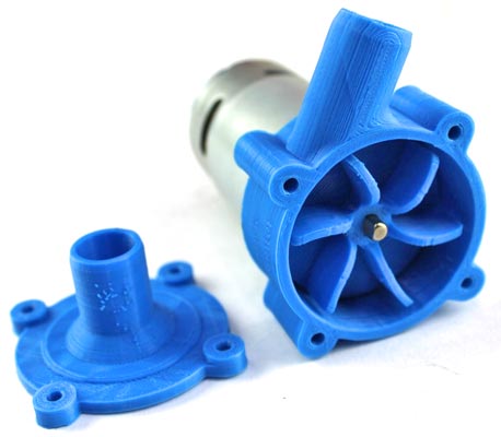
Removable Casing: It is a type of casing where we remove the motor whenever it is not needed because it uses the Nut-bolt mechanism, making assembling and de-assembling easy. Its biggest advantage is using the same motor for other projects. Also, any blockage inside the casing set can be easily cleaned.

The STL design file includes Outer Casing and Impeller designs which can be downloaded using the Link.

Water Pump Casing Design

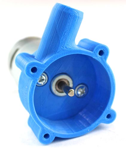
After 3d-printing, our structure is looking as below Image.

3D Printed Water Pump Casing

Non-removable Casing: In this type of casing, the outer part is completely glued using Araldite after the proper fitting of the impeller. It is a permanent solution; we can’t remove the motor at all.

The STL design file can be downloaded using Link.

Non-removable Casing Design

After 3D Printing, our structure is looking as below Image.

3D Printed Non Removable Casing

Assembly & Functioning

A centrifugal water pump is a mechanical device that circulates and moves water through pipes by creating force in one direction.

A water pump required basic few necessary components for work. Let’s study the included components and their functioning:

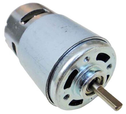
  1. 775 Motor: This commonly available DC motor offers high torque and power output. It runs on a 12-volt to 24-volt power supply. The motor/engine provides the necessary energy to rotate the impeller and generate the required pressure to move the water.
  2. Impeller: A fan-like component that will be attached to the motor shaft to create water movement. It consists of curved blades or vanes that are designed to push the water in a specific direction when the impeller spins.
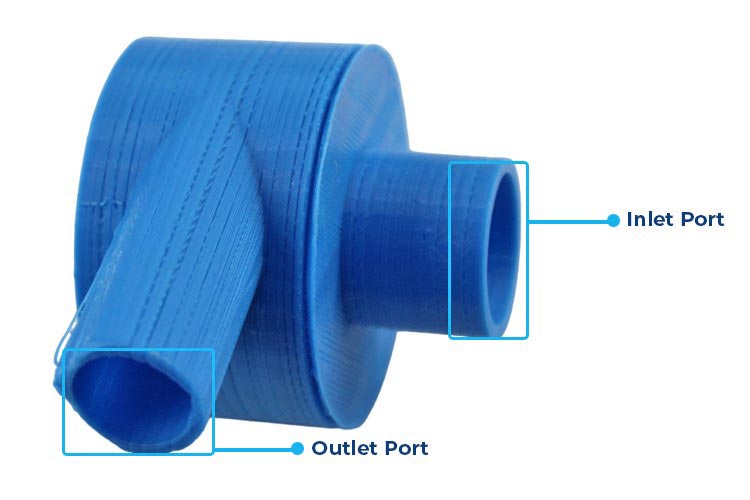
  3. Housing/Casing: The housing or casing is the outer shell of the water pump, usually made of durable materials. It encloses all the internal components and provides support and protection. The 3D casing has two ports—an inlet and an outlet. The inlet port allows water to enter the pump, while the outlet port is where the pressurized water exits the pump.

3D Casing of Water Pump

  1. Suction Pipe: The suction pipe is connected to the inlet port and is responsible for drawing water into the pump.
  2. Discharge Pipe: The discharge pipe is connected to the outlet port and carries the pressurized water away from the pump to the desired location.
  3. Power Supply: A suitable DC power supply to operate the motor (e.g., a 12V battery or power adapter).
  4. Screws, Nuts, and Bolts: For securing the motor, impeller, and other components.

Assembling and Connection of the Removable Water Pump

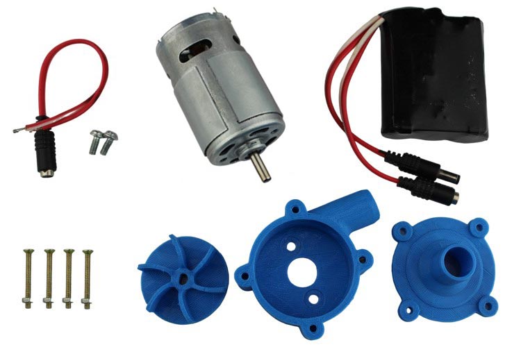
It is quite easy process & doesn’t take much time. Below Images give a brief Idea of the Required Components.

Removable Water Pump

Let’s look at the step-by-step procedure:

Screwed the back fittings of the case to the motor using an M4-10mm bolt shown in the image below.

  • The “M” designation for metric screws indicates the outer diameter of the screw in millimeters, so for an M4 screw, the outer diameter is 4mm.
  • The head is a standard star head and the length of the screw is 12mm.

12mm screw

After the proper fitting, the case will look like this:

Take the impeller, whose center has a D-shaft hole to prevent slipping during high torque, and fix it to the motor shaft.

impeller

If your motor shaft is circled-shaped, then you can try to file the rotor shaft from the outer side to transform it into D-shape, or else if you can find it, you can directly purchase it. The motor 775 that I am using is also circled in shape, hence I used a Grinder machine to file its shaft.

775 motor

After, the impeller fitting the structure will look like this:

3d printed casing

Now, attached the front side of the casing using the M3-30mm bolt, as shown in the below image.

  • Outer Diameter is 3mm
  • Length is 30mm

M3-30mm bolt

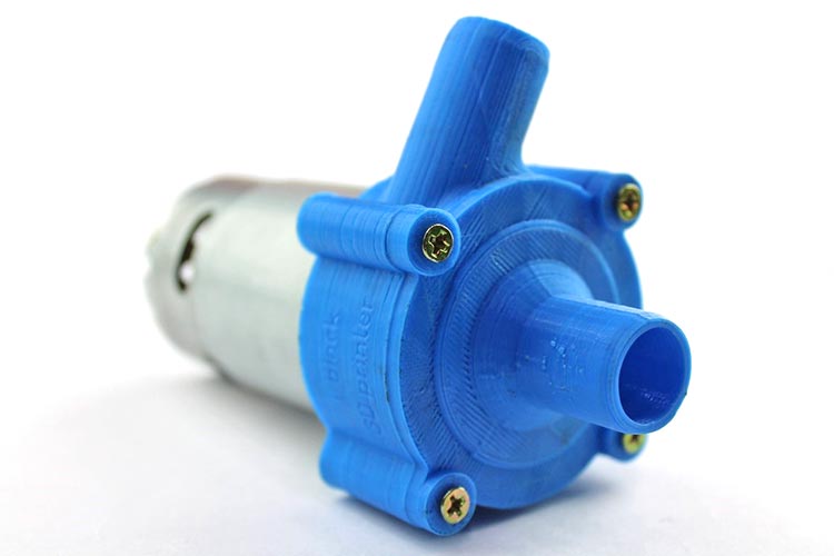
After all the fitting, the complete structure will look like the below image.

3d printed casing on 775 motor

Take the DC female connector Jack soldered it to the two output pins of the motor.

Note: Be careful about the right polarity to set the clockwise spinning direction of the motor because the wrong direction spinning will not generate the water flow with full efficiency.

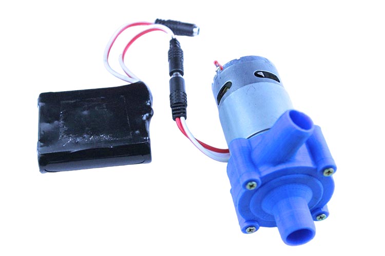
Connect the 12-volt battery supply (or you can use up to 24-volt), and see how the pump is working. We capture an image to demonstrate the pump.

3d printed casing water pump with battery

Assembling and connection of the Non-Removable water pump

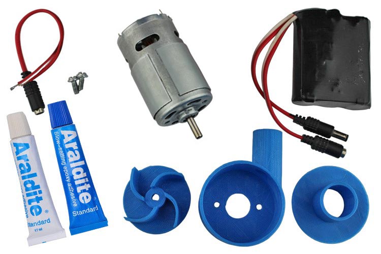
The necessary Required component is shown in the Below image. Some of the components are the same as in the case of Removable water pump. Hence, some of the steps are the same as previous one.

Non-Removable water pump components

The same M4-10mm bolt is also used here to Screw the back fittings of the casing to the same 775 motor. For more details about the screws, you can refer to that step.

After the fittings, the casing will look like this:

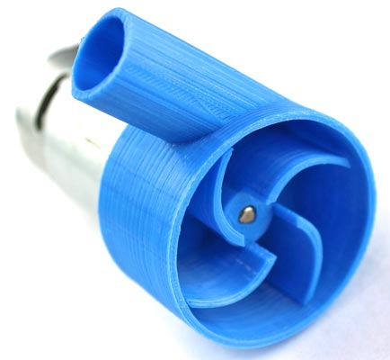
Take the D-shaft impeller, and gently pushed to fix its hole into the D-shaft of the motor.

3d printed casing assembly

Apply the Araldite Glue at the round edges and fix the front side casing. Make sure the glue is properly set without any air leak spaces.

3d printed casing assembly on 775 motor

Soldered the DC female jack at the input pins of the motor by carefully observing the anti-clockwise spinning direction.

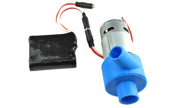
We connected the 12-volt battery and test the spinning direction and functionality of the motor.

3D Printed Non Removable Casing on Water Pump

Demonstration & Testing

We have completed all pump fittings, remaining only the connection to a power source, and required some water-filled buckets.

As a power source, I am using a 12-volt Lithium-ion battery, you can also use a 12-volt adaptor, or else you can use up to a 24-volt power source.

Inlet/outlet suction Port sizes

  • For Removable Casing: The external diameter should be 18mm (as per the STL file) for both inlet and outlet ports.
  • For Non-Removable Casing: The inlet port should have an external diameter of 25mm whereas the outlet port has of diameter 20mm (as per the STL file).

The functioning of a water pump involves the following steps:

Priming: Before starting the pump, it needs to be primed to remove any air trapped inside the system. Priming involves filling the pump and suction pipe with water to create an airtight seal and ensure proper water flow.

Power Input: The motor or engine is started, providing the necessary rotational force to the driveshaft. We are using a 12-volt supply to power the motor.

Impeller Rotation: As the driveshaft rotates, it drives the impeller to spin rapidly inside the housing. The impeller's curved blades push the water outward from the center of rotation.

The rotation direction of the impeller is depending on the motor rotation direction. For, Removable pump it should be clockwise whereas for Non-removable it should be anticlockwise.

Water Intake: The rotating impeller creates a low-pressure zone at the inlet port, causing water to be drawn into the pump through the suction pipe. The water flows into the housing and towards the center of the impeller.

Impeller Action: The impeller blades propel the water radially outward with centrifugal force, increasing its pressure as it moves toward the outer edges of the impeller.

Water Discharge: The pressurized water exits the pump through the outlet port and flows into the discharge pipe. The pressure generated by the impeller's action allows the water to be transported to its intended destination.

Continuous Operation: The water pump continues to operate as long as the motor or engine is running, maintaining a steady flow of water and circulation throughout the system.

We learned the functioning and mechanism of the water pump and now it’s time to test and see the live working.

The Above GIF shows the live working of a Removable water pump whereas the below shows the working of a Non-removable pump.

The motor torque is enough to provide a sufficient water flow at a 12-volt power source but if You want to get high force torque, you can go with a 24-volt power source with a speed of up to 50-60 liters/min.

Hope you enjoyed the Project and learned something useful from it. If you have any questions, you can leave them in the comment section below.

Have any question realated to this Article?

Ask Our Community Members

How to Build a NAND Gate with Transistors?

Submitted by Gourav Tak on
Here is everything you need to know about NAND Gates, how they work, and how to build one yourself.
Have any question realated to this Article?

Ask Our Community Members

Why Global Semiconductor Firms are in Dilemma to Increase the Output of Wafer Fabs

The top-notch technology will provide a huge impetus to the R&D initiatives, but the major impediment is the lack of wafer fabrication at this level.

A recent survey report by Counterpoint Research highlighted that in 2022 the growth in revenue of international semiconductor wafer fabs augmented to 9 percent year-on-year, worth $120 billion. Experts added that this is staggering growth because for the past couple of years, there has been a massive imbalance in the logistics sector, massive shortages of components, currency undulation, and most importantly, macroeconomic slump. But, the situation proved to be very optimistic for the wafer fabs owing to the huge investments by the customers in the mature node devices across numerous segments such as 5G, AI, automotive, HPC, and IoT. Suppliers, which are at the top five, witnessed a huge profit of $95 billion in their services and systems.

While speaking of the revenue of the wafer fab equipment’s market, it is anticipated to reduce by 10 percent year-on-year to $108.45 billion after a continuous growth in the past three years. Although the market for WFE in 2023 does not look promising, the prospect of Extreme ultraviolet lithography (EUV) lithography looks quite promising due to continued deployment of EUV into logic and memory. Not only that, foundries all over the world are increasing manufacturing chips of 3-nm nodes by utilizing FinFET architectures and Gate-All-Around transistors along with escalated adoption of EUV technology.

Dale Gai who is the associate director at Counterpoint Research opined that over the last couple of months, TSMC has started working on innovative capacities in in 7/6nm and 5/4nm owing to the decreased demand in the market, but the capital and the investment on 3-nm process nodes remains almost same like it was planned in the first half 2023. The point to be noted is that during the time of COVID-19 pandemic, various segments of the semiconductor industry have witnessed soaring prices because of the huge disruption in the supply chain. On the other hand, the electric vehicle technology is gaining a huge momentum and therefore, the entire automobile industry has seen a surging growth.

Nonetheless, the unexpected increasing demand of semiconductors during the time of pandemic has caused prices to augment in the data center and industrial market. The slow growth has also happened due to the inflation, which has reduced the orders for consumer electronic goods, and mobile phones. The expansion of AI, start-ups, and other technologies are happening on a rapid scale, the requirement of microchips are also increasing throughout the world.

semiconductor manufacturing

Recession is another major obstacle currently among various industries, which has forced semiconductor companies to take into consideration whether they should increase the output of wafer fabs or not. The current skills in manufacturing and end-to-end design are magnetizing the interests of various businesses across the globe. The top-notch technology will give a huge impetus to the R&D initiatives, but the major impediment is the lack of wafer fabrication at this level. Building a wafer fab requires huge investment and is very expensive and also needs gallons of water which is why there are not many fabs available currently. Here, government incentives and subsidies will play an imperative role and the Chinese government has already assured to invest around USD 73 billion as semiconductor subsidies, while Japan, US, and Europe failed to equate that amount.

In the past three quarters, no major investment unifications have been done and therefore every country is investing on their own without proper analysis and knowledge. As consumers now require more top-notch devices, the production must be increased to a larger extent, feel experts. There are about 150 300-mm fabs located, with 12 in Europe and Middle East, 33 in China, 42 in Taiwan, and 19 in the US. This is why the volume of supply as per the demand is still unnatural. The massive level of production and activity still happens at the 200-mm fab with demand being the same for various nodes starting from 90nm to 180nm processes. The total number of 200mm fabs all over the world is 230 with 49 in the Middle East and Europe and 51 in the US.

The question here appears to be why the WFE market increases every year. As per a previous report of CircuitDigest, various characteristics such as the escalating demand from the consumer and B2B electronics industry coupled with ever-increasing technological improvements in the semiconductor and telecom industry are speculated to spearhead the demand for the semiconductor wafer fab equipment market from 2019-2030. There are some additional factors like equipment and silicon wafer that would assist in analyzing the concerned market in the coming years. Most importantly, new-fangled innovation in wafer technology has crafted a denser packaging of devices like transistors and MEMS (micro-electro-mechanical system) are speculated to create a way for the foundation of innovative opportunities that can be leveraged by various global firms.

Now, speaking of the current wafer fab market globally, in 2021 the market was worth USD 62930 million and by 2030, the market is expected to reach at USD 97470 million at a CAGR of 5.6 percent between 2022-30, according to a report of capital market firm MarketWatch. But, another research firm Verified Market Research added that in 2021, the WFE market reached at USD 68,989.03 million and by 2030, it is expected to grow USD 164,669.67 Million at a CAGR of 8.04 percent between 2023-30. The technological developments over the past few years have spearheaded the growth of this sector. The growth in memory storage capacities and the augmenting compactness of numerous communication products in the telecom industry are responsible behind this growth.

global wafer equipment market graph

Going by the detailed analysis, the WFE market is divided into Latin America, Europe, North America, and Asia Pacific. In 2021, the biggest market share in this segment was grabbed by the Asia Pacific region and is expected to increase at a CAGR of 8.53 percent in the forecasted period. The region is leading because of the fact that there are solid supply chains of semiconductor devices such as discrete devices, circuits, and logic circuits across nations like China, Taiwan, and Japan. As there is a huge growth in consumer electronics and automotive products, the demand for IC chips and SIC wafers are also expected to increase.

Other than that, there are huge volumes of suppliers in South Korea and in India, who are contributing to the huge growth of this market. In the same year, North America stood as the second biggest region and during that time it was predicted that this region is likely to contribute massive growth. But huge subsidies, and incentives offered by the government of the Asia Pacific region has helped them to lead the market. Increasing demand along with rising income, growth of advanced machinery and technology, and programs for spreading the importance of the requirement will help the WFE market to grow immensely over the years.

Counterpoint’s Senior Research Analyst Ashwath Rao said, “Considering the growth in terms of US dollar, the overall volume of WFE market slumped by around 8 percent in 2022 as it was negatively impacted by currency fluctuations, and especially reduction in value of euro and yen denominated sales ever since the starting of 2022. Ahead of the inflection in 2022, there is an escalation in R&D investment that has put the WFE market to outperform the semiconductor market for a long term.

Highlighting the overall scenario of the market in 2023, Rao mentioned in a survey report, “Manufacturers are more skewed towards foundry-logic segments today unlike in 2019, and with overall backlog strength, increased visibility in terms of long-term agreements and subscription model will help limit the downside. The weakness in wafer fab equipment spending in 2023 will drive lead time and inventory normalization. The slowdown in memory-oriented investments will begin to recover gradually starting in the second half of 2023, and 2024 will be a big year for the equipment industry. Manufacturers are well positioned to take advantage of the opportunity."

Have any question realated to this Article?

Ask Our Community Members

How to Build an XOR Gate with Transistors?

Submitted by Gourav Tak on

In the vast world of digital electronics and logic circuits, The XOR gate stands as a fundamental building block that plays a crucial role in information processing. XOR, short for Exclusive OR. Is a logical operation that produces an output of high when the number of high inputs is odd, and low when the number of low inputs are even. This unique characteristic makes the XOR gate an essential component in various applications, ranging from simple binary arithmetic to complex data encryption algorithms.

In this article, we will explore the inner working of the XOR gate, including its truth table, logical symbol representation, circuit diagram, and practical  construction using transistors.

Previously, we have built many electronic circuits to perform logic gates like XOR Gate, NAND Gate, NOT Gate, NOR Gate, AND Gate, OR Gate, XNOR Gate

What is an XOR Logic Gate?

The XOR gate is also called the exclusive OR gate. An electronic XOR gate performs the digital logic XOR function. This function is generally similar to the standard OR function with one critical difference. For both OR and XOR, the output is high when either of the two inputs are high, and when both inputs are low, the output is low.

However, when both inputs are set to a high state, the standard OR circuit will produce a high output signal, whereas the XOR circuit will generate a low output signal. This fundamental behavior is the reason behind it is called exclusive OR gate. In the simplest design of XOR gate only 5 transistors are needed.

XOR Gate Symbol

XOR Gate Symbol

Truth table of XOR gate

Inputs

Output

A

B

Y

0

0

0

0

1

1

1

0

1

1

1

0


Boolean expression for this gate is

Y = (A ⊕ B)

Output

(A ⊕ B) = A.B + A.B

The truth table above shows clearly demonstrates that the output of an Exclusive-OR gate will only goes “HIGH” when both of its two input terminals are at different logic levels with respect to each other. If these two inputs, A and B are both at logic level “1” or both at logic level “0” the output is a “0”.

Logic Diagram of XOR Gate

Logic diagram of XOR gate

As can be seen in the logic diagram above, the Ex-OR gate is built by combining three different types logic gates, the OR gate, the NAND gate and the AND gate to produce the desired result.

Components Needed for building XOR gate

So with just the few components, we can construct a XOR gate circuit.

  • 2N2222 (NPN) transistors x5
  • 10kΩ resistors x3
  • 220Ω resistors x3
  • Push buttons x2
  • Breadboard x1
  • 9V Battery x1
  • LEDs and Connecting wires

Circuit Diagram of XOR Gate using Transistors

The circuit diagram below illustrates the XOR gate using 5 NPN transistors. Here, I1 and I2 represent the two inputs, and O1 signifies the output.

Circuit Diagram of XOR Gate using Transistors

The picture shows a simple XOR gate circuit that uses 5 transistors. In the layout inputs A and B are both connected to 9V supply. Different color connecting wires help to see the connections. If there is any ambiguity in the placement of wires the circuit diagram can be referenced.

The gate design is a NAND gate on the left two transistors, a switch for the middle transistors, and an OR gate for the last two transistors.

Circuit of XOR Gate with Transistors

Upon examining the configuration shown in the photo, it becomes evident that the current generated by the far-right resistor is unable to reach the ground on the lest, resulting in the LED remaining off. The reason behind this lies in the fact that all the current generated by the first resistor on the left is directed towards the first ground. Consequently, the switch remains in the off position due to insufficient voltage entering the base of the third transistor.

In the event that one input is activated, the current gains ability to flow from the far-right transistor to the second ground. Finally, when both inputs are deactivated, the output remains off since the current fails to enter the base of the OR gate transistors. this configuration prevents the current from traveling from the far-right resistor to the second ground.

Applications

From the depth of cryptography to the realm of error detection, the XOR gate proves to be an indispensable ally. It possesses the power to perform bitwise operation, enabling binary addition and subtraction, ensuring data integrity, and even generating parity checks. This gate’s versatility and elegance have solidified its role in countless digital system, paving the way for technological advancements that shape our modern world.

Have any question realated to this Article?

Ask Our Community Members

A Simple DIY Bluetooth Audio Player using Wireless Hi-Fi Amplifier Module

The Bluetooth Amplifier Module is useful for DIY projects for creative and hobbyists. The module’s Bluetooth connectivity makes the project connect wirelessly and gives hustle-free entertainment. The board can work on Lithium-ion/Li-Po or Lead Acid battery, which is used to make the device portable. Its design makes it easy to implement the module for projects that are handy, cheap, and provide High Sound Quality.

You can build your own DIY Bluetooth Music Player using Audio Amplifier to use at home/office, or while traveling.

In this project, we will learn the connections and circuitry of the Module. Also, gather some necessary information and Technical Specifications.

Circuit Digest have built many audio circuits, check out the huge collection of audio circuits with schematics and detailed explanation, to help you build Audio projects and use them for your Audio designs. Also check previously built DIY music player:

Wireless Hi-Fi Bluetooth Amplifier Module

Wireless HI-FI module is a Class AB / Class D switching function, 5.3W output power single channel audio power amplifier Board with Built-in Bluetooth, FM, USB, aux cable, and memory chip decoder support.

Wireless Hi-Fi Bluetooth Amplifier Module

With its comprehensive set of input ports and impressive features such as compactness, attractive design, and high audio quality, this module stands out from other boards. Its versatility makes it a preferred choice for various applications.

  • A power switch to turn ON/Off the module.
  • A micro-USB charging connector at fixed 5-volt input.
  • AUX-Cable 2.5 mm female Input Jack.
  • USB card, TF card Input ports.
  • Inbuilt Bluetooth & FM Support.
  • A Multi-Purpose Functioning Switch.
  • It has two inbuilt Red & Green LED indicators [see their functionality later].

The module has a lot more internal options for supporting other features. The module also has two Open connections to connect MIC and an extra LED for power indication, as indicated in the below diagram.

Bluetooth Amplifier Module Parts Name

  • Connecting an extra LED to the Board will not be effective as it only indicates the ON/OFF status according to the power switch.
  • Soldering a small piece of wire to the FM Antenna Terminal will make the signals and audio quality better while in FM Mode.
  • Connecting MIC is very helpful & Futuristic for your project. It allows you to talk on calls during the module connected to the smartphone via Bluetooth or AUX.

Bluetooth Amplifier Module Speaker and Battery Connector

Bluetooth Audio Amplifier Circuit Diagram

DIY Bluetooth Music Player Circuit Diagram

Let’s have a look at the comprehensive circuit connections of the Board which are very straightforward & simplest design to understand.

Connect the Battery to the battery connector of the module. You can use a 3.7-volt lithium-ion Battery or a 4-volt Lead Acid Battery.

Battery Input-voltage Range: Using this Module, we can able to see the battery draining percentage in our Smartphone. This function purely works based on the Remaining battery voltage which is sensed by the controller IC.

  • At 3 volts, it shows the battery fully drained [0%] while at 4.2-volts it sensed the battery as fully charged [100%].
  • We can give up to 5 volts to the battery terminals of the module to boost the audio quality performance of the audio IC.

Note: This module can also work with the direct power of a Micro-USB charging Connector whose input is fixed at 5 volts without any battery.

Speaker Matching Specifications

The Module uses a HAA2018 audio IC whose Vdd range is 2.5-5.5 volts. It is a Class AB / Class D switching function, 5.3W output power single channel audio power amplifier IC whose Technical Specification are:

Class D output power:                  

  • 5.3W (VDD=5.0V, RL =2Ω,THD+N=10%)
  • 3.2W (VDD=5.0V, RL =4Ω,THD+N=10%)

Class AB output power:               

  • 5.2W (VDD=5.0V, RL =2Ω,THD+N=10%)
  • 3.1W (VDD=5.0V, RL =4Ω,THD+N=10%)

The RL denotes the Load Impedance whereas the VDD is the battery terminal voltage to the audio IC.

Others Features:

  • Low distortion and low noise
  • Start-up POP sound suppression function
  • Shutdown current is less than 1uA
  • Overheat protection function

Since, from the above technical specification, you can be aware that at 2Ω Load impedance, the output power will be highest. If you can find 2Ω 5w Speaker, then it will be well & good otherwise you have to set a Series/parallel combination of speakers to match the impedance and power rating according to the output rating of the Amplifier module. In general, it is advisable to match both the impedance and power ratings when connecting speakers and amplifiers. If possible, it is recommended to use a speaker with an impedance that matches the amplifier's output impedance. Additionally, selecting a speaker with a power rating equal to or higher than the amplifier's output power will provide better performance and reduce the risk of damaging the components.

Since our Amplifier output rating is 2Ω 5w, hence I am using two 4Ω 2.5w speakers in parallel connection which is equivalent to the Amplifier output.

Amplifier and Speaker Connection Diagram

Let’s have a look at the real circuit prototype in the below image

Bluetooth audio amplifier Circuit

Demonstration of Bluetooth Audio Amplifier Board

We have already seen the connection details above, and now we get an insight into the functioning of such a kind of Board like how its indicators work differently in different modes.  

  • Connect the lithium-ion battery properly by taking care of +ve & -ve correct terminals. Also, connect the speakers with the correct matching for proper audio quality.
  • Turn-On the switch and check for a Blue blinking LED.

Mode and LED Indicator

The Module works in different Five types of Modes, these are Bluetooth, FM, AUX, Pendrive, and SD-card Mode. The Blue LED indicator indicates a bit differently in each mode, making it easy to understand the internal functioning of the board.

Bluetooth Mode: The module is always in BT mode by default after turning ON the Board.

  • The Blue Led blinks fastly until the BT will not be paired.
  • Led Continuous ON after pairing or while pausing the song.
  • Blinks Slowly while playing the Song.

FM Mode: Holding & pressing the multi-function button towards the center will change the mode to FM.

  • The Blue Led blinks fastly until all the channels will not be scanned.
  • Blinks Slowly while playing a channel.

USB/SD-card Mode: The module will automatically initiate the USB-drive mode when you plugged in a USB-Drive.

  • Led Continuous ON while pausing the song or if there is no song inside the memory drive.
  • Blinks Slowly while playing the Song.

Note: Mp3 songs must be present in the Flash drive otherwise it won’t Access the USB drive.

AUX Mode: Connect an AUX cable to provide audio input to the board from Smartphone.

  • Always Blinks Slowly while playing/pausing the Song.

Charging Functionality

It has a Micro-USB input port to charge the Battery pack attached to the Module. There is a Red Led to indicate the charging mode of the module. The Red Led is continuously glowing while battery charging.

Charging voltage at battery terminal: 4 volts

Charging current: ∼200 mA

Note: Don’t charge the device while using it because it will not charge your battery.

Bluetooth audio amplifier Circuit

Hope you enjoyed the project and learned something useful from it. If you have any questions, you can leave them in the comment section below.

Have any question realated to this Article?

Ask Our Community Members

Raspberry Pi Pico W Bluetooth: C/C++ and MicroPython Update

The Raspberry Pi Pico W is a versatile microcontroller board that packs a lot of power into its compact form factor. With the integration of Wi-Fi and Bluetooth capabilities, it opens up a world of possibilities for projects that require wireless communication.

Bluetooth C/C++ SDK Support

To make use of Bluetooth on the Pico W, the latest version of the Pico SDK (1.5.0) introduced Bluetooth functionality that was previously unavailable. This update brings various Bluetooth libraries that expand the capabilities of the Pico W when it comes to utilizing Bluetooth technology.

Here's an overview of the available Bluetooth libraries for the Raspberry Pi Pico W:

Bluetooth Classic: This library enables communication using traditional Bluetooth technology. It allows you to connect and communicate with other devices that support Bluetooth Classic, such as smartphones, computers, and other microcontrollers.

Bluetooth Low Energy (BLE): BLE is a power-efficient variant of Bluetooth designed for low-power devices. It enables you to create energy-efficient applications that can communicate with other BLE-enabled devices, such as fitness trackers, smartwatches, and IoT devices.

Bluetooth Sub Band Coding (SBC) encoding/decoding: This library provides audio encoding and decoding capabilities using the SBC codec. With this feature, you can stream audio wirelessly between the Pico W and other Bluetooth-enabled devices, such as speakers or headphones.

Bluetooth Network Encapsulation Protocol (BNEP) support using LwIP: BNEP support allows you to encapsulate network traffic over Bluetooth connections using the Lightweight IP (LwIP) stack. This feature enables you to establish network connections and exchange data between the Pico W and other Bluetooth devices.

Bluetooth Network Encapsulation Protocol (BNEP) support using LwIP with FreeRTOS for NO_SYS=0: This library offers BNEP support specifically for systems using the FreeRTOS operating system with the NO_SYS=0 configuration. It allows you to use BNEP over Bluetooth connections while leveraging the benefits of FreeRTOS.

These Bluetooth capabilities on the Raspberry Pi Pico W open up exciting possibilities for various projects. For example, you can create applications that involve audio streaming, where the Pico W acts as a Bluetooth audio source or receiver. You can also implement volume control functionality to adjust audio levels wirelessly. Additionally, you can explore projects that turn the Pico W into a Bluetooth keyboard or mouse, allowing it to interact with other devices.

To get started with Bluetooth on the Raspberry Pi Pico W, you'll need to follow the Pico SDK's quick-start instructions. These instructions provide guidance on setting up the necessary software tools and libraries to utilize Bluetooth features on the Pico W. Additionally, the Pico SDK documentation includes numerous Bluetooth examples that can serve as a reference for your own projects.

Note: - The Bluetooth support for pico W on Arduino IDE has yet not been confirmed or arrived.

Micropython Support

While MicroPython support for Bluetooth on the Pico W has not been officially released yet, there are indications that work is underway. Jim Mussared, the founder of MicroPython, has acknowledged the demand for Bluetooth support and mentioned active development efforts. This suggests that MicroPython support for Bluetooth on the Pico W may become available in the near future. To stay updated on the progress, you can monitor the relevant GitHub thread where the development is being discussed.

Once MicroPython support for Bluetooth is added to the Pico W, it will further enhance the accessibility of Bluetooth capabilities for a wider range of developers and enthusiasts. This will unlock even more exciting possibilities for creative projects, as it will enable developers to leverage the simplicity and ease of use offered by MicroPython while utilizing Bluetooth features on the Pico W.

In conclusion, the Raspberry Pi Pico W's integration of Wi-Fi and Bluetooth capabilities brings immense potential for wireless communication and opens up new avenues for innovative projects.

Have any question realated to this Article?

Ask Our Community Members

How US WIll Lead The Global Wireless Market Amid Tough Challenges

US government must provide a crystal-clear strategy when spectrums will be available so that businesses, operators, component and hardware providers can prepare themselves before utilizing these spectrum.

The industry association Cellular Telecommunications and Internet Association (CTIA) hosted the 5G summit on May 17, 2023, in Washington DC where numerous bigwigs from the US government and the wireless industry assembled to discuss the monumental improvement in unleashing the 5G networks and the new use-cases. At the event, the officials also discussed the pending works that need to be done and the grave impediments, which the industry is facing. Devoid of any skepticism, there is a sense of positive vibes about the new opportunities that 5G promises to bring, but many believe that it is still in the early stages. The industry leaders have opined that for a successful 5G penetration, policymakers must look forward for more incentives, schemes, and also support it.

During the event, a plan has been chalked out by the speakers about how much improvement has been made on 5G and by all measures, it has been made clear that it is the fastest deployed wireless generation yet. Now, if we speak about the mmWave frequencies, low-band, and mid-band, AT&T, Verzon, and T-Mobile cover 320 million US citizens. The unleashing of mid-bands have been very fast, while AT&T’s senior vice president of Engineering and Operation, Egal Ilbaz highlighted that the company will be able to reach 200 million Point of Presence (PoPs) towards the end of 2023, while on the other hand, Neville Ray, President of Technology, T-Mobile stated that their firm would be able to reach 300 million PoPs.

Why The Federal Communications Commission Allowing Additional Spectrum for 5G Services?

A year back, the FCC has made high-band spectrum auctioning a top priority. The first 5G spectrum auctions have been done in the  28 GHz band; the 24 GHz band; and the upper 37 GHz, 39 GHz, and 47 GHz bands. The Commission along with these auctions is also allowing 5 gigahertz of 5G spectrum into the market and is also undertaking efforts to free up 2.75 gigahertz of 5G spectrum in the 26 and 42 GHz bands. Additionally, the FCC has taken a step for more useful utilization of additional millimeter-band spectrum in the 70/80/90 GHz bands. According to a report of FCC's official website, Mid-band spectrum has become a target for 5G buildout given its balanced coverage and capacity characteristics. With their work on the 2.5 GHz, 3.5 GHz, and 3.7-4.2 GHz bands, they will make more than 600 megahertz available for 5G deployments. And speaking of the low-band, the FCC is acting to improve use of low-band spectrum (useful for wider coverage) for 5G services, with targeted changes to the 600 MHz, 800 MHz, and 900 MHz bands.

Speaking of the 5G infrastructure policy in the US, they must be updated by the FCC so that more investments can be made in the 5G ecosystem. Chairwoman of the FCC, Jessica Rosenworcel told the global media, "If we want broad economic growth and widespread mobile opportunity, we need to avoid unnecessary delays in the state and local approval process. That’s because they can slow deployment.” In an effort to promote digital opportunity for every US citizen, the outmoded regulations will be modernized by the FCC. The 5G fund for rural US has been established by the FCC in October 2020 so that they can have around $9 billion in Universal Service Fund by which the operators will be able to set-up cutting-edge 5G mobile wireless services in the rural USA, which also includes $680 million for deployment on the tribal lands.

Back in 2022, the FCC had commenced bidding auction of mid-band spectrum and that bidding auctioned around 8,000 county-based licenses in the 2.5 GHz spectrum band in mostly the rural region of America. According to an exclusive report of Reuters, AT&T Inc led bidders in the 3.45 GHz mid-band spectrum auction, winning $9.1 billion, while T-Mobile won $2.9 billion and Dish won $7.3 billion. FCC C-Band spectrum auction last year, three of the biggest US wireless firms won $78 billion in bids. For 3,511 licenses, Verizon Communications paid $52 billion, while T-Mobile grabbed $9.3 billion, and AT&T grabbed $23.4 billion in licenses.

The Ongoing Challenges Of The Wireless Industry And What’s Next For 5G

5G technology has already transformed the consumer’s lives in various ways, but according to the experts, bigger organizations will benefit more from this technology as it has the potential to power connected irrigations, smart cities, factories, and many more. Now, the executives from DISH, Verizon, T-Mobile, and AT&T were all highlighting the flexibility and the opportunities that virtualized, software-powered networks would provide benefits for developers in the organization. The low-latency AI and ML applications will be deployed seamlessly for efficiency by distributed computing at the edge. The situation is also a bit pessimistic because in the enterprise level, the 5G development is slow and the foggy economic ecosystem would prevent some organizations from experimenting and deploying 5G to perk-up their productivity.

But, as the unleashing of mid-bands is happening soon, 5G will be able to benefit the enterprise to improve their outputs. During the 5G summit, the speakers have made it clear that Chinese operators are going to fulfill 25,000 orders for the private networks. Although the US is a bit behind in this scenario, which will obviously change in the coming few years. The problem of digital divide can be countered by the wireless industry. The arrival of fixed wireless access (FWA) offers a replacement for the fiber, which will be low-cost in various parts of the world while offering the required capacity and speeds to connect rural areas, thereby improving trade, education and various other sectors.

Even though 5G is furnished with numerous opportunities, there are some strict hurdles that are preventing this technology from reaching its potential. Experts claim that the ongoing high level of geopolitical tensions between China and the US is an imperative factor. Also, the executives from Ericsson and Samsung have stated that the state subsidies provided by the Chinese government for its infrastructure firms makes it very intricate to compete on the price, which forces numerous nations to go for Chinese wireless network providers.

Matthew Orf, the US based research analyst at Counterpoint Research said, "The Government of China’s Aggressive business strategy for unleashing 5G has given the country a chance to spearhead the wireless industry and chinese network providers and organizations are having a huge experience in deploying new use cases before the western nations. This is ultimately offering the Chinese firms a tremendous competitive advantage in regards to their western rivals.

Now, if we look towards 6G, the geopolitical tussles between China and the US is going to negatively impact the entire global wireless market, which would also decrease the interoperability and scale. Therefore, America must work closely with its allies throughout the world to have a single standard out of which everyone can benefit,” added Orf.

Orf also highlighted that in an effort to counter these hurdles, the industry leaders called the US policymakers to give more authorization to the FCC to open spectrum auctions and provide more spectrums for the operators. This is because the volume of data consumption is augmenting very rapidly, while more spectrum is also required for the new enterprise use-cases. But, this authorization to the FCC is not enough and the US government must provide a crystal-clear strategy when spectrums will be available so that businesses, operators, component and hardware providers can prepare themselves before utilizing these spectrums.

Have any question realated to this Article?

Ask Our Community Members

How to make a Gyroscope?

Have you ever wanted to try building your own gyroscope? Well, you're in luck! In this blog post, we'll guide you through the steps to make a gyroscope using just a few simple materials.

How does a Gyroscope work?

A gyroscope is a sensor that measures and maintains orientation and angular velocity. It is commonly used in various applications such as navigation systems, robotics, aerospace, and virtual reality devices.

The math behind a gyroscope has to do with how it stays upright. When you spin the small CD attached to the motor, it starts to spin really fast. This creates something called "angular momentum," which is like a special kind of energy that makes things spin around.

Gyroscope Circuit on CD

The bigger CD is attached to the small CD and motor, so it also starts to spin around. This makes the whole gyroscope spin around as well. But even if you move the gyroscope around, it stays upright because of something called "torque."

Torque is a special kind of force that makes things rotate. When you move the gyroscope around, it experiences torque that causes it to rotate around a different axis. The rate of precession is proportional to the amount of torque applied and the angular momentum of the gyroscope.

The equation for torque is

T = I * α,

Where T = torque applied,

I = moment of inertia (a measure of how difficult it is to rotate an object), and

α = angular acceleration.

So in simpler terms, the faster the small CD spins and the bigger the CDs are, the harder it is to move the gyroscope around because it has a lot of angular momentum.

I hope that helps make it easier to understand!

What you’ll need:

  • 1 small DC motor
  • 1 big CD
  • 1 counterweight
  • 1 9V battery
  • 1 switch
  • Hot glue or double-sided tape
  • Small bolt (optional)

Attach CD to Motor

Attach CD to Motor

First, take the CD and attach it to the DC motor in the way which is shown in the image above. You can do this using some hot glue or double-sided tape. Make sure the CD is centered on the motor's shaft so that it will spin smoothly.

Attach Counter weight to Motor Shaft

Attach Counter weight to Motor Shaft

Next, take the counterweight and attach it to the shaft of the motor. You can use a small bolt or some more hot glue to secure the motor shaft to the counter weight. I have used a wheel as a counterweight but it’s not necessary. You can use anything which has a symmetrical shape as the counterweight, but you need to do some trial and error.

Circuit Diagram

Gyroscope Circuit Diagram

Now it's time to wire everything up! First, connect the switch to the 9V battery. Then, connect the positive wire from the battery to the positive terminal on the motor. Connect the negative wire from the battery to the negative terminal on the motor.

Test Your Gyroscope

Once everything is wired up, you can test out your gyroscope by turning on the switch. The motor should start spinning the smaller CD, and the larger CD should rotate around it. You've just created your very own gyroscope!

Experiment!

One of the coolest things about gyroscopes is their ability to maintain their orientation and rotation even when they're disturbed. You can experiment with your gyroscope by tilting it to one side and watching it slowly right itself. Try using different sizes and shapes of CDs to see how they affect the gyroscope's behavior.

Building your own homemade CD gyroscope is a fun and educational project that you can do in just a few hours. Try to make this project and tell us what you learned!

Projects using DC Motor

Control DC Motor with Arduino and L293D Motor Driver IC

Explore the exciting world of robotics and learn how to control DC motors with Arduino and the versatile L293D Motor Driver IC. In this blog post, we'll guide you through the step-by-step process of setting up the motor driver, connecting it to your Arduino board, and programming it to control the speed and direction of your DC motors. Unleash your creativity and bring your robotic projects to life with this essential knowledge!

Low Power SMS Based Vehicle Tracking System with A9G GSM+GPS Module and Arduino
Simple H-Bridge Motor Driver Circuit using MOSFET

Take a deep dive into motor control as we unveil the secrets of constructing an efficient H-Bridge motor driver circuit using MOSFETs. Our comprehensive blog post will guide you through the circuit building process, shed light on the underlying principles of H-Bridge operation, and empower you to effortlessly control the direction and speed of your DC motors. Expand your technical expertise and unleash the true potential of motor control in your projects with this invaluable knowledge.

Interfacing DC Motor with AVR Microcontroller Atmega16

Are you ready to take your motor control skills to new heights? Join us as we delve into the exciting world of interfacing DC motors with the powerful AVR Microcontroller Atmega16. In our insightful blog post, we'll guide you through the entire process, from establishing a seamless connection to programming the Atmega16 for precise control over the speed and direction of your DC motors. Discover how this integration opens up endless possibilities for your projects, allowing you to unleash the true potential of motor control. Get ready to elevate your technical prowess and create remarkable innovations with AVR Microcontroller Atmega16 and DC motors.

Have any question realated to this Article?

Ask Our Community Members