How to Generate Sine, Triangle, and Square Waves Using ICL8038?

Today we are looking at one of the affordable frequency generator modules, that has ICL8038 as its heart. Surprisingly it is capable of generating 3 different types of waves which are Square, Sine, and Triangle. There is a lot about this module that needs to be discussed, so without further ado, let us jump into the explanation of the ICL8083 Module.

What is ICL8038?

The ICL8038 is a simple and versatile waveform generator IC that can produce sine, square, and triangle waves with just a few external components. It’s great for generating signals in various applications, with a frequency range from 0.001Hz to 300kHz. You can easily adjust the frequency using resistors and capacitors, and even control frequency modulation with an external voltage. It's built to perform reliably across different temperatures and voltage ranges, making it a practical choice for signal generation. The image below shows the clear image of the ICL8038 Module.

ICL8083 Module

Features of ICL8038

  • Low frequency drift with temperature: 250 ppm/°C

  • Low distortion (sine wave output): 1%

  • High linearity (triangle wave output): 0.1%

  • Frequency range: 0.001Hz to 300kHz

  • Adjustable duty cycle: 2% to 98%

  • Supports high-level outputs from TTL to 28V

  • Outputs sine, square, and triangle waves simultaneously

Specification of ICL8038 Frequency Generator Module

Below, you can see the general specifications of the ICL8038 module.

ParameterSymbolLimitsUnit
MinTypicalMax
Module Supply VoltageVss101230V
Module CurrentIs-1220mA
Output FrequencyFo0.00110 - 300K480KHz
Duty Cycle-3-90%
Operating TemperatureTo-50-150°C
Storing TemperatureTs-65-150°C

The table above is for beginners. If you are looking for more advanced details, refer to the official ICL8038 Datasheet.

The most important factor here is the input voltage. I recommend using a constant input voltage if you expect a consistent waveform, as the output waveform changes its properties such as frequency and amplitude, whenever the input voltage fluctuates.

To be precise, the data sheet itself states the maximum frequency of 300 kHz but this module can pump up to 480 kHz which under testing produces unstable frequency with lower amplitude than regular.

Hardware Overview

Let's take a deeper look at the hardware itself. Given its complexity, we will break down the details into multiple subtopics. 

ICL8083 Module Components

We'll begin with the pinouts.

Pinouts of ICL8038 Module

In the ICL8038 module, the pinouts are straightforward. You need to power it, and the desired waveform of your chosen configuration can be obtained from the output. Below, you can see the pinout image and the table that describes the pinouts of the ICL8038 module.

ICL8083 Module Pinouts

Pin NoPin NameTypeDescription
1VCCPowerModule Supply Voltage
2GNDPowerGround Connection Pin
3AGAnalog OutputThe output pin that's best suited for receiving the sine and triangle waves.
4GPowerGround Connection Pin
5DCDigital OutputThe output pin that's best suited for receiving the Square waves.

The supported input voltage range is approximately 10 to 30V maximum. However, 30V is not recommended as it will eventually increase the operating temperature. An optimum of 12V is suggested for better operation.

The output can be drawn in two forms: one as a pure analog wave and the other as a DC-biased voltage. Each has its unique advantage. Analog output is best suited for sine wave output, while DC output is best suited for triangle and square wave outputs.

Next, we will continue with the configurations.

Configurations available in ICL8038 Module

Typically, there are two configurations available in the ICL8038 module: frequency range selection and waveform type selection. The image below shows the exact shunt jumper positions that need to be adjusted to select the correct configuration, along with a small table describing the available configurations.

ICL8083 Module Configurations

Part No

Part Name

Description

1

5 way - Shunt JumperFor Configuring Frequency Range

2

3 way - Shunt JumperConfiguring Output Wave Type

One thing to remember is that selecting the correct frequency range is important to achieve the desired output. Ideally, try to position the desired frequency in the middle of the range to allow smooth adjustments and ensure a stable output. For example, if you need 100Hz, a range of 10Hz to 450 Hz is suitable. If you need 100kHz, a range of 6kHz to 120kHz is recommended.

Finally let's look at the controls available to tune the wave form.

Controls Available in ICL8038 Module

This module has all the major tuning options, allowing us to easily modify the signal’s waveform. Below, you can see the part-marking image of all the components that assist in tuning the signal, along with a table representing each control option and its scope of operation.

ICL8083 Module Waveform Controllers

Part No

Part Type

Controllable Waveform

Description

1

Trimmer Potentiometer

All

Duty Cycle Adjustment

2

All

Frequency Adjustment

3

Square Wave

Linear Regulation

4

All

Output Amplitude Adjustment

5

Sine Wave

Linear Adjustment

Here is some information I would like to add,

Duty cycle adjustment, frequency adjustment, and amplitude adjustment are common for all types of waveforms. However, linear regulation or adjustment is an additional feature for square and sine waves.

Except for amplitude adjustment, every other control has some influence on the signal's frequency. So, be cautious when setting the correct frequency for your application.

Schematics of ICL8038 Module

Finally, here is the schematic, which is essential for understanding, recreating, or modifying the ICL8038 module. Below is the complete schematic diagram of the module.

ICL8083 Module Schematics

Starting with the Power Section, the input voltage is passed directly to the circuit without any regulation. Before reaching the circuit, the voltage goes through two filter capacitors to prevent surges. Additionally, there's a power indicator LED near the input.

You can also adjust the frequency of the output waveform by altering the input voltage at the FM Sweep Pin of the ICL8038. This changes the charge and discharge timing of the capacitor, affecting the output frequency.

There are two separate circuits to adjust the waveform: one for sine wave linearity and another for duty cycle adjustment. Specifically, you use the R13 potentiometer to fine-tune the linearity of the sine wave and the R12 potentiometer to adjust the duty cycle of all waveforms.

Finally, we have the Output Section. The module generates three waveforms simultaneously (sine, square, and triangle). You can select the desired waveform using a shunt jumper(P2). The selected waveform is amplified by a general-purpose NPN transistor (Q1). The amplitude can also be adjusted using the R14 potentiometer. Additionally, the R15 potentiometer, connected to the base, is used to adjust the linearity of the square wave that doesn't affect other waveforms..

For the outputs, the module provides two options—AC and DC. Typically, DC output is preferred for square and triangle waveforms, while AC output is more suitable for sine waveforms. You can choose the appropriate output based on the selected waveform and your specific needs.

Next Let's see about the Controlling and its Relative Output.

Guide Tuning the Output Signal

Here, I will show all the configuration and tuning options along with the output recorded from the oscilloscope. As we know, there are three different waveforms, and among these, there are four different controls, except for the triangle waveform, which has three controls. Starting with the sine waveform.

Remember: Every GIF has two signals, one in yellow and another in blue. The yellow signal is the DC output, while the blue signal is the analog output. All footage is taken while providing 12V to the ICL8083 module. The GIFs are recorded while rotating the respective potentiometer.

SineWave - Amplitude Adjustment

Below is the waveform captured while adjusting the amplitude trimmer potentiometer. As you can see, we get an approximate output range of 320 mV to 5.12 V with an input voltage of 12 V. Although the DC output (yellow wave) appears similar to the AC wave, the key difference is that the analog output has a proper offset over the signal period, while the DC output is most likely a true DC output.


Therefore, it is recommended to use the analog output for the sine wave.

SineWave - Frequency Adjustment

It is generally observed that adjusting the potentiometer changes the frequency within the selected range. However, if you turn the potentiometer to either end, the output will be null. It is better to keep the potentiometer in the middle position. Additionally, the frequency is not stable at the ends of the potentiometer's range.


SineWave - DutyCycle Adjustment

There is generally no need for duty cycle adjustment in a sine wave. However, here is what happens when you adjust the duty cycle while in sine wave configuration.


Ensure that the duty cycle is set to approximately 50% to maintain a proper sine wave.

SineWave - Linearity Adjustment

In the sine wave configuration, adjusting the linearity allows you to modify the timing between the positive and negative cycles.


In most cases, it should be kept close to 50%. Only under special conditions would you need to adjust the linearity to either end.

TriangleWave - Amplitude Adjustment

Now we switched to the triangle wave form output. Here Amplitude adjustment is as usual. And similar ranges of voltage like sine wave has observed.


In the GIF above, you can clearly see that the DC output (yellow wave) provides the best triangle waveform. Therefore, it is best to use the digital bias output for the triangle wave.

TriangleWave - Frequency Adjustment

As with the sine wave, adjusting the frequency of the triangle wave produces similar results.


Also, remember to avoid tweaking the ends of the potentiometer, as the output will be null at those extremes.

TriangleWave - DutyCycle Adjustment

An interesting observation is that while adjusting the duty cycle in the triangle wave configuration, you can obtain two additional waveforms: the positive ramp and negative ramp.


In the GIF above, you can see three types of waveforms, the sawtooth negative ramp, the triangle wave, and the sawtooth positive ramp.

SquareWave - Amplitude Adjustment

In the square wave configuration, the DC output (yellow wave) provides a more appropriate square waveform. Therefore, it is suitable to choose the DC output for the square wave.


Regarding the output voltage range, we successfully achieved 320 mV to 7.6 V, which is slightly higher than the sine wave. As usual, a 12V input voltage is given to the module.

SquareWave - Frequency Adjustment

Similar to the other waveforms, the result is the same when adjusting the frequency of the signal.


SquareWave - DutyCycle Adjustment

Here, I have a slight disappointment because, as shown Below GIF video, the output signal does not cover the duty cycle range specified in the datasheet of the ICL8038 IC. which is 2% to 98%.


So, some fine-tuning of the circuit might be necessary.

SquareWave - Linearity Adjustment

While adjusting the linearity of the square wave signal, we observe that it only affects the amplitude of the signal. The purpose of this adjustment is unclear, as we already have a separate potentiometer for adjusting the amplitude.


Application of ICL8038 Frequency Generator Module

Due to its ability to generate multiple types of waveforms, there are a variety of applications. Let's explore a few,

  1. Signal Generation
    Used as a function generator to create sine, square, triangle, sawtooth, and pulse waveforms for testing and troubleshooting circuits.

  2. Modulation System
    Helps generate carrier signals for Amplitude Modulation (AM) and Frequency Modulation (FM) systems. It is also useful for testing communication circuits.

  3. Audio Testing
    Useful for generating audio signals to test speakers, amplifiers, and audio processing circuits.

  4. Oscillator Circuits
    Acts as a tunable oscillator in electronic circuits that require a variable frequency source.

  5. Waveform Analysis
    Assists in simulating and analyzing different types of waveforms in research, teaching, and laboratory setups.

  6. Pulse Width Modulation (PWM)
    With adjustable duty cycles, it can be used in applications requiring PWM control, such as motor control or dimming LEDs.

Have any question realated to this Article?

Ask Our Community Members

Semiconductor Manufacturing Companies in India: Current State and Future Forecasts

Overview of India's Semiconductor Industry: India is on a transformative path to become a important player in the global semiconductor market. As the world’s fifth-largest economy, India is pushing towards self-reliance in manufacturing, especially in the semiconductor sector. With an ambitious vision set by Prime Minister Narendra Modi, the country aims to grow its electronics sector from a current valuation of $155 billion to a stunning $500 billion by 2030. This vision underscores the importance of establishing semiconductor plants in India to produce semiconductor devices and meet domestic and global demand.

Importance of Semiconductor Plants: Semiconductor plants are essential for producing the chips that power everything from laptops and smartphones to advanced machinery and electric vehicles. Given the increasing demand for technology in daily life and various industries, establishing plants for semiconductor manufacturing in India is vital. These plants not only strengthen domestic production, but they also reduce reliance on imports and contribute to economic growth and job creation.

Current State of Semiconductor Manufacturing in India

Raise_Of_Chip_Growth_In_India

Background of Semiconductor Manufacturing in India: The semiconductor manufacturing journey in India has been relatively emerging. The country has primarily relied on imports for its semiconductor needs, with a significant percentage of chips sourced from established players like China and Taiwan. Despite this, India's landscape is changing and the government is focused on developing a strong semiconductor ecosystem to meet both domestic and international demands.

Current Market Size and Growth: As of 2023, the Indian semiconductor market value is approximately $34.3 billion which is projected to grow to $100.2 billion by 2032 as per the expert analysis. This growth reflects a compound annual growth rate (CAGR) of around 20.1%. Such expansion indicates an increasing reliance on semiconductors across various sectors, particularly with the rise of electric vehicles, IoT devices and advanced communication technologies.

Government Initiatives and Policies

Government Policies: The Indian government has recognized the strategic importance of semiconductors and has rolled out various initiatives to boost domestic manufacturing. Policies such as the "Development of Semiconductors and Display Manufacturing Ecosystems in India" aim to provide the necessary structure and incentives for semiconductor plants to thrive. The manufacturing experts have highlighted the benefits of the India's new schemes and policies for the electronics industry in a recent interview with industry specialists. This initiative aims to make India as a universal electronics hub, with an allocation of Rs. 2,30,000 crore (approximately USD 30 billion). It supports semiconductor plants in India including display fabs, silicon fabs and semiconductor packaging, highlighting trusted sources for national security. Additionally, the program includes a design-linked incentive scheme to encourage startups, creating skilled job opportunities and enhancing India's integration into the global value chain. 

Investment Strategies and Funding Initiatives: The Indian government is heavily investing in the semiconductor industry to strengthen domestic manufacturing. As part of its strategy, financial incentives have been introduced, covering up to 50% of plan costs for companies that are setting up semiconductor plants in India. This initiative is designed to attract global tech companies and encourage local manufacturing. The Union Cabinet has approved the establishment of three new semiconductor plants, which are expected to create 20,000 job opportunities directly. Additionally, these projects could generate indirect employment opportunities for up to 60,000 people, benefiting a broad range of related industries.

Collaborative Efforts with Other Countries: India is also building partnerships with various countries to boost its semiconductor manufacturing skills. Working together with nations like the Taiwan and U.S. is essential to learn how to create advanced semiconductor plants and for gaining the new technology. For instance, the Micron Technology, American chipmaker is planning to introduce its first semiconductor chip plant in India by 2025. This highlights how important it is to have international teamwork in this field.  

Moreover, India is keen on learning from established semiconductor hubs. Collaborations may involve sharing knowledge, training programs and joint research initiatives that can lead to innovation. The Indian government is actively seeking to attract global players to invest in these projects, which will not only enhance technical capabilities but also create job opportunities for the nation’s workforce. Overall, these efforts are crucial for India to position itself as a competitive player in the global semiconductor landscape.

Key Semiconductor Manufacturing Plants in Development

With government-approved status, the following are the top listed semiconductor manufacturing companies in India and overseas that are currently developing new plants to expand their production capabilities, with several plants under construction expected to begin production by the end of 2024 and the beginning of 2025. 

Key_Fabs_in_Development
  • Tata Electronics and Powerchip Semiconductor Manufacturing Corp (PSMC) - Dholera, Gujarat 
    Tata Electronics is partnering with Taiwan’s Powerchip Semiconductor to build India’s first large-scale semiconductor fab in Dholera. With an investment of ₹9,100 billion (around US$109 billion), the plant will focus on producing high-performance computing and power management chips. The facility aims to produce 50,000 wafers monthly to meet the demand in sectors like electric vehicles and telecommunications.

  • Tata Semiconductor Assembly and Test Pvt Ltd (TSAT) - Morigaon, Assam
    In Morigaon, Tata Semiconductor Assembly and Test Pvt Ltd (TSAT) is establishing an advanced packaging facility. With an investment of ₹2,700 million (around US$326 million), this ATMP unit will cater to industries such as automotive, consumer electronics and telecommunications, helping to reduce India’s reliance on imported semiconductor components.

  • CG Power and Renesas Electronics Corporation - Sanand, Gujarat
    In Sanand, Gujarat, CG Power is collaborating with Japan’s Renesas Electronics and Thailand’s Stars Microelectronics to set up another ATMP unit. This ₹760 million (about US$91 million) project will focus on producing specialized chips for sectors like consumer electronics and automotive, with a daily capacity of 15 million chips, strengthening India's semiconductor capabilities.

  • Micron Technology - Sanand, Gujarat
    Micron Technology is building a semiconductor unit in Sanand, Gujarat, which is advancing quickly. The facility is set to produce memory and storage chips starting in 2025. This project, costing $2.75 billion, is backed by $825 million from Micron and additional funding from the government. The focus will be on creating products mainly for export, helping to strengthen India’s position in the global semiconductor market.

  • Kaynes Semicon - Sanand, Gujarat
    Kaynes Semicon is developing an OSAT (Outsourced Semiconductor Assembly and Test) unit with a ₹3,307 crore (US$400 million) investment. Partnering with global firms like LightSpeed Photonics and AOI Electronics, this facility aims to produce 1 billion chips annually within five years, with a strong focus on power electronics and industrial applications.

  • Suchi Semicon - Surat, Gujarat 
    Suchi Semicon is set to commence production at its advanced OSAT facility in Surat by November 2024. With an investment of ₹3,000 crore, this hi-tech plant features Class 10k and 100k cleanrooms and aims to create 1,200 jobs while focusing on cutting-edge semiconductor assembly and testing technologies to support various industries. In a recent interview with Suchi Semicon's Managing Director, Mr. Ashok Mehta, he shared his vision for boosting India’s semiconductor design capabilities and highlighted the important role the company aims to play in this process.

  • Foxconn-HCL Joint Venture (Pending Approval)
    This proposed OSAT unit by Foxconn and HCL Group is currently awaiting final approval. The facility aims to utilize Foxconn's expertise in electronics manufacturing.

  • ASIP and Korea’s APACT (Pending Approval)
    A joint venture between ASIP Technologies and Korea’s APACT is also pending approval for an OSAT facility in Sanand. The focus of this plant will be on system-in-package (SiP) technologies.

  • Tarq Semiconductors (Pending Approval)
    Tarq Semiconductors, a company owned by the Hiranandani Group, is seeking approval for an ATMP facility and a compound semiconductor unit. This project is intended to enhance India's capabilities in advanced packaging and compound semiconductor production.

Global Context and Competition

India's goal to become a leader in semiconductor manufacturing comes among strong competition from global giants like Taiwan, China, South Korea, the U.S. and Japan. Taiwan dominates the market with around 44% of the global share, followed by China at 28%. These countries have well-established semiconductor industries with decades of experience. To compete effectively, India must rapidly develop its manufacturing capabilities while learning from the successful strategies and technologies of these major players. Collaborations, technological advancements and government support will be key for India to find a significant role in the global semiconductor industry.

Collaborations and Partnerships

International Collaborations: India's strategy includes building international collaborations to enhance its semiconductor manufacturing capabilities. The ongoing partnership with Taiwanese companies like PSMC and collaborations with U.S. firms reflect the need for India to leverage global expertise and technology.

U.S. and India Partnerships: The U.S. has expressed strong interest in partnering with India to expand its semiconductor sources and reduce dependence on Taiwan and China. Recently, the U.S. Department of State announced a partnership with the India Semiconductor Mission to improve the global semiconductor value chain. This collaboration is expected to strengthen both countries positions in the semiconductor landscape, especially in ongoing geopolitical risks.

Economic and Employment Impact

Economic_and_Employment_Impact
  • Job Opportunities: The establishment of semiconductor plants in India is expected to create a large number of jobs across various sectors. By 2026, it's estimated that over 300,000 job opportunities will be available, covering roles such as engineers, testers, software developers and operational staff. These jobs will not only support semiconductor production but also open up employment in connected fields, helping local talent grow in technical and managerial positions. This flow in job creation is vital to utilizing India’s young workforce, driving both economic growth and skill development.

  • Positive Effects on Related Industries: The growth of the semiconductor industry will positively impact other sectors like automotive, electronics and telecommunications. As semiconductor manufacturing expands, these industries will see increased demand for components and new technologies, leading to innovations in their products and services. Additionally, companies working in research and development (R&D) will be able to explore advanced technologies, creating more opportunities for investment and collaboration. The overall result will be a boost to multiple industries as they adopt cutting-edge technologies, enhancing India’s technological part.

  • Economic Growth: Constructing of semiconductor manufacturing plants in India will also contribute to strengthening the country's economy. By increasing its manufacturing capacity, India can focus on producing components for export, which will integrate the nation more deeply into global supply chains. This effort is part of India’s broader plan to increase its share in the global technology market. As semiconductor manufacturing grows, it will lead to more investment, higher productivity and economic growth, helping India become a hub for advanced manufacturing on the global phase.

Future Outlook and Challenges

Market Forecasting: India's semiconductor industry is projected to grow rapidly over the next decade. From $34.3 billion in 2023, it is expected to reach $100.2 billion by 2032, driven by demand from sectors such as electronics, automotive and telecommunications. Experts of India highlight the importance of a resilient supply chain to support this growth, particularly in strengthening the electronics industry for global competitiveness. Initiatives like “Make in India” and “Digital India” are boosting this growth by encouraging domestic production and innovation. As India's digital economy expands, the demand for semiconductor products will increase, particularly in advanced technologies like AI, IoT and 5G, positioning the country for substantial market potential in the global semiconductor landscape.

Challenges: Despite the promising outlook, India faces several challenges in its semiconductor journey. Building the necessary infrastructure, acquiring advanced technology, and attracting foreign investments are key hurdles. India’s semiconductor industry is in its early stages, and establishing a strong manufacturing base requires significant capital, expertise and time. Furthermore, global competition from countries like Taiwan and China, which dominate the semiconductor space, presents an additional challenge. To succeed, India must continue to invest in its semiconductor ecosystem, improve its technological capabilities and create a favorable business environment for both local and foreign players.

For India to successfully position itself as a global semiconductor hub, attracting more foreign investments will be essential to finance the capital-heavy semiconductor fabs. The country also needs to enhance its technological capabilities to keep pace with established global leaders. Improving the business environment is another crucial step, including simplifying regulations, offering incentives and promoting innovation. These initiatives will not only assist growth but also ensure that India becomes a competitive player in the global semiconductor landscape, driving innovation and economic development in the coming years.

Conclusion

Key Findings: India is making significant strides toward becoming a leading player in the semiconductor industry, driven by government initiatives, international collaborations and the establishment of key semiconductor plants. With ambitious goals for growth and development, the country's semiconductor landscape is set for a transformation.

Final Thoughts: The increase in chip manufacturing companies in India presents a unique opportunity for the nation to enhance its technological capabilities, create job opportunities and contribute to economic growth. By leveraging its strengths and addressing existing challenges, India can strengthen its position in the global semiconductor value chain and pave the way for a brighter future in technology.


Have any question realated to this Article?

Ask Our Community Members

New Tech Tuesdays: Choosing Reliable Power Supply for High-Tech Applications

Submitted by Staff on

Join Rudy Ramos for a weekly look at all things interesting, new, and noteworthy for design engineers.

In today's digital era, power is essential for operating our technological infrastructure. Whether through AC or DC electricity, it sustains vital functions across homes, businesses, hospitals, educational institutions, and industrial manufacturing, ensuring seamless operation for all. Without power, technology as we know it ceases to operate, so securing reliable power sources is imperative for sustaining our progress and fostering innovation.

While all these power uses are essential, some are more critical than others. Certain business-critical applications demand the most reliable power sources. When it comes to the need for high-performance power supplies, the XP Power HPF3K0 AC-DC Power Supplies stand out. These power supplies are integral to demanding applications like medical imaging, semiconductor manufacturing, and advanced industrial equipment, where extreme precision, reliability, safety, and efficiency are paramount.

In this week’s New Tech Tuesday, we'll explore the features and benefits of the XP Power HPF3K0 series and why it's ideal for these advanced applications.

The Newest Products for Your Newest Designs

The XP Power HPF3K0 AC-DC Power Supplies series is packed with cutting-edge features that make it a top contender in the power supply market. The HPF3K0 series is designed to meet various high-tech industries' stringent and business-critical needs. The highly flexible, digitally controlled HPF3K0 series offers up to 3kW of power density from four variants with nominal single output voltages of 24, 36, 48, and 60VDC. Moreover, for applications requiring more power, up to five power supply units wired in parallel via a single wire bus may current share, providing up to 15kW of highly flexible power (Figure 1).

Upto 5 HPF3K0 Power Units Connected Together

Figure 1: Up to five power supply units can be paralleled simultaneously with current share accuracy ±3 percent of a single unit maximum current rating. (Source XP Power)

At the core of this versatile power solution lies a digital signal processing “engine” equipped with advanced control and monitoring capabilities. This enables dynamic adjustment of power configurations and performance, featuring constant current and constant voltage operation, variable overload characteristics, and alarm functions.

Medical Imaging Applications

The healthcare manufacturing sector requires stringent safety certifications. XP Power’s HPF3K0 power supply solutions meet these high standards to ensure patient safety and well-being, making them the preferred choice for precise and reliable power supply in medical imaging systems.

Medical imaging equipment, such as magnetic resonance imaging (MRI) and computed tomography (CT) scanners, demands precise power delivery to function accurately. The HPF3K0's stable output voltage ensures that imaging devices operate smoothly, providing clear and accurate results. Consistent power is crucial in medical diagnostics to avoid artifacts or errors in imaging, which can lead to misdiagnosis or the need for repeat scans.

The HPF3K0 series meets IEC60601-1 Ed. 3 standards with 2×MOPP (Means of Patient Protection) and is approved to EN55011/EN55032 for EMC Class B (conducted) and Class A (radiated), and EN61000-4-x for immunity. It also holds ITE IEC62368-1 Ed. 2 approval.

Semiconductor Manufacturing Applications

Semiconductor manufacturing is another industry where the HPF3K0 series shines. Its robust design and high efficiency make it perfect for powering complex semiconductor equipment and fabrication processes.

Semiconductor manufacturing involves processes that require stable and precise power. Power variation can lead to defects in semiconductor wafers, which can be costly and time-consuming. The HPF3K0 features the programmable constant current and constant voltage needed for equipment used in delicate semiconductor manufacturing processes, ensuring high-quality production (Figure 2).

Semiconductors

Figure 2: Semiconductor equipment manufacturers rely on stable process power to ensure precision, repeatability, and reliability in their equipment, thereby minimizing wafer defects and enhancing yield. (Source: xiaoliangge/stock.adobe.com)

The HPF3K0's user-defined digital controls and alarms help reduce downtime and improve overall productivity in semiconductor manufacturing plants. Its high efficiency contributes to lower energy costs and reduces environmental impact, aligning with the industry's goals for sustainable manufacturing.

Tuesday’s Takeaway

XP Power's HPF3K0 AC-DC Power Supplies series combines digital control and configurable functionality in a compact, high-efficiency, and robust design, perfect for demanding business-critical applications. Its digital architecture, scalability, high power density, and comprehensive medical safety approvals highlight its exceptional features, making it an ideal choice for medical, semiconductor manufacturing, and advanced industrial equipment applications.

Original Source:  Mouser

About the Author

Rudy is a member of the Technical Content Marketing team at Mouser Electronics, bringing 35+ years of expertise in advanced electromechanical systems, robotics, pneumatics, vacuum systems, high voltage, semiconductor manufacturing, military hardware, and project management. As a technology subject matter expert, Rudy supports global marketing efforts through his extensive product knowledge and by creating and editing technical content for Mouser's website. Rudy has authored technical articles appearing in engineering websites and holds a BS in Technical Management and an MBA with a concentration in Project Management. Prior to Mouser, Rudy worked for National Semiconductor and Texas Instruments.

Have any question realated to this Article?

Ask Our Community Members

How smart farming solutions are manufactured in India? | Mobitech Wireless Solutions | Tech Tour

Smart farming is revolutionizing the farming industry by incorporating technology into standard practices. Mobitech Wireless Solutions located in Tamil Nadu is leading this transformation by offering solutions that improve productivity and sustainability. In this article will delve into how Mobitech is reshaping the landscape of smart farming with its advanced products and technologies.

How to build AI and Machine Learning Projects Using Maxduino

In a previous article, we looked into the Maixduino Development kit and learned how to use it with the Arduino IDE. In this article, we will learn how to use Micropython in the Maixduino development kit. First, we will learn how to flash the Micropython firmware to the Maixduino and then how to set up Sipeed’s Maixpy IDE and use AI and Machine Learning with the board.

What is MaixPy?

MaixPy is a port of Micropython specifically for the K210 SoC. It not only supports generic MCU functions but also integrates hardware-accelerated AI machine vision and microphone array-related algorithms. Keep in mind that the Maixduino supports the MaixPy V1, but there is another version of MaixPy called MaixPy V4 which is for the newest Sipeed product called MaixCam and doesn’t support Maixduino. The main benefit of using MicroPython is that it is much easier and faster to do development. So let’s start with the basics and learn how to prepare the Maixduino board to use with MaixPy.

Installing the USB driver

As we know the Maixduino features two SoCs onboard a K210 AI SoC and an ESP32-Wroom Module. Since both of these doesn’t have any native USB support, the manufacturers used a USB to UART bridge for communication and firmware updates. Since we need two separate UARTs for the SoC, Sipeed chose a custom solution that uses a CH552 MCU with dual serial firmware. By doing this they were able to implement the communication between the computer and both of the onboard SoCs through a single USB port. Since they are using a custom solution, it is necessary to install any required drivers for it to be able to communicate with the computer.

In a Linux environment, we don’t need to install any drivers. The operating system will automatically detect the hardware and assign a generic driver that is already a part of the Linux system. All we need to do is note the port numbers. For that open the terminal window and type the following command ‘ls /dev/ttyUSB*’ and hit enter. A list of available USB devices and corresponding ports will be displayed. Note down the appropriate port number for further use. In Windows, it is necessary to install the specific driver. For that go to the USB driver download page, and download the driver file. There will be multiple files on the download page. The easier method would be to download the zip file with the setup in the name, extract it, and run the driver installer. It will automatically install the driver. Another way is to download the driver files from the download page and manually install the driver from the device manager. Once the driver is successfully installed and the MAxiduino is connected to the computer, open the device manager and expand the Ports (COM and LPT) section. You will find two comports that will be shown only when the Maxiduino is still connected to the PC. Note down the port number, by default the first port number will be for the K210 SoC and the second will be for the ESP32.

Installing the MaixPy firmware

So before coding, we must install the Maixpy firmware to the Maxiduino so that it will accept the micropython code and execute it. For the first make sure you have installed the driver as per the instruction above and note down the port number. In Linux and Mac OS execute ls /dev/ to see the port numbers and in Windows use the device manager. So to start with we need to download the precompiled firmware file. For that first go to the MaixPy firmware page. In there, select the latest version folder and in it, you will find multiple firmware files with either .bin or .kfpkg extensions. Use the following table to select the appropriate firmware for your application. Once selected download the firmware binary to your computer

File name

Remark

maixpy_*.bin

Normal firmware, with

* basic api

* kmodel V4 support

* no LVGL support

* NES emulator support

* AVI format video support

* IDE support

maixpy_*_minimum.bin

Minimal function firmware, with

* basic api

* only few OpenMV's APIs, some APIs like find_lines are not included

* only kmodel V3 support

* no LVGL support

* no NES emulator support

* no AVI format video support

* no IDE support

maixpy_*_minimum_with_kmodel_v4_support

Minimal function firmware with

* add kmodel v4 support

maixpy_*_openmv_kmodel_v4_with_ide_support

Minimal function firmware with

* add kmodel v4 support

* IDE support

maixpy_*_minimum_with_ide_support.bin

Minimal function firmware with

* IDE support

maixpy_*_with_lvgl.bin

Firmware with lvgl support, including

* basic api

* only kmodel V3 support

* LVGL support

* NES emulator support

* AVI format video support

* IDE support

maixpy_*_m5stickv.bin

Firmware especially for the M5StickV board, with functions the same as the normal firmware

maixpy_*_amigo*.bin

Firmware especially for the Amigo board, with functions the same as the normal firmware

Once the firmware file is downloaded, the next step is to download the firmware flashing utility. For flashing or upgrading the firmware we are going to use the kflash_gui, for that download it from the kflash_gui download page. Extract the firmware and run the kflash_gui application. For Windows, it is recommended to run it using “run as administrator”.

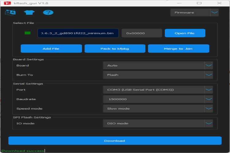
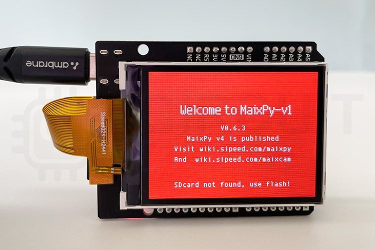
Once the app is opened select the previously downloaded firmware. As you may observe the address range will be automatically populated and you don’t need to change it. Select the proper COM port(by default the first COM port of the two that will appear when the board is connected.) and click on download the flash utility will flash the firmware to the board and once it's done the board will reset and the MaixPy splash screen will be displayed on the LCD display.

Installing the MaixPy IDE

The next step is to install the MaixPy IDE. For that go to the MaixPy IDE download page and download the appropriate binary for your operating system. For Windows run the installer as usual and follow the onscreen instructions. For Mac use the DMG file and install the application. For Linux use the following commands to give permission and to install the IDE.
chmod +x maixpy-ide-linux-x86_64-0.2.2.run
./maixpy-ide-linux-x86_64-0.2.2.run

Once installed open MaixPy IDE, and select the model of the development board in the Tool menu. And click on the connect button in the bottom left corner of the IDE window. It will automatically connect to the Maixduino board.

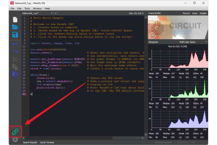
When opening the IDE for the first time it opens with a test code already in it. So to test the code just click on the Run button located below the Connect button as shown below. The code will be loaded into the Maixduino board and executed. The example code initializes the camera module and display and continues to display the video stream from the camera on the display. You can also see the video preview in the MaiixPy IDE.

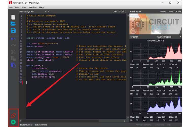
To stop running the code click on the stop button(same as the run button). To upload the files to the board use the Send file option from the Tools menu.

Using the Maixduino With Serial Terminal

After flashing the MaixPy firmware we can also use the Maixduino through any serial terminal without the need of the IDE if needed. For this, we can use any serial terminal that we are comfortable with, for example in Windows we can use Putt, mobaxterm , xshell , or mpfshell-lite and in Linux we can use the pyserial. The MaixPy IDE itself has a built-in serial terminal and we can also use that too. Sipeed recommends mpfshell-lite and more details about how to use them can be found on the mpfshell-lite page. If we want to run a micropython script, open the serial terminal, press CTRLl+E and paste the following code

import sensor, lcd

sensor.reset()
sensor.set_pixformat(sensor.RGB565)
sensor.set_framesize(sensor.QVGA)
sensor.run(1)
sensor.skip_frames()

lcd.init(freq=15000000)

while(True):
    lcd.display(sensor.snapshot())

Press Ctrl+D on the keyboard to start running the code. In the code, you can see that we imported the necessary libraries for the camera and display using the import function. Later we initialised the camera and configured it. After that, we have initialised the display. Then using the while loop we display the live video feed from the camera on the TFT display.

Maixduino File System

The Maixduino has a total of 16MB of onboard storage and an SD card slot for external storage. The file system structure of the Maixduino is illustrated in the image below. 

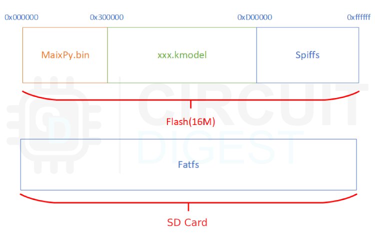
The internal storage is divided into three parts: namely the MaixPy.bin firmware area, the xxx.kmodel model area, and the file system area. As the name suggests the MaixPy.bin area is for the MaixPy firmware storage and the xxx.kmodel area usually starts at 0x300000 and is used for the trained AI model. For the generic filesystem, the Maixduino uses SPIFFS. The SD card must be formatted with FATFS for the Maixduino to be able to access it. If the trained model is larger than the xx.kmodel area, we can also use the SD card to store it.

Managing the File System and Uploading the Code

As we know in micropython all the scripts are stored as .py files, to modify the scripts it is necessary to have filesystem access for creating, editing or deleting those files. So with Maixduino, we have multiple ways to do these file handlings. The first method includes using the Micropython Editor (pye) editor which is built into the MaixPy firmware. We can use the serial terminal for the Pye editor. You can use os.listdir()to view the files in the current directory and pye("hello.py")to create a file and enter edit mode. After editing the file you can press Ctrl+S to save, and Ctrl+Q quit editing. You can find more details about the Micropython editor on the Micropython editor GitHub repo.

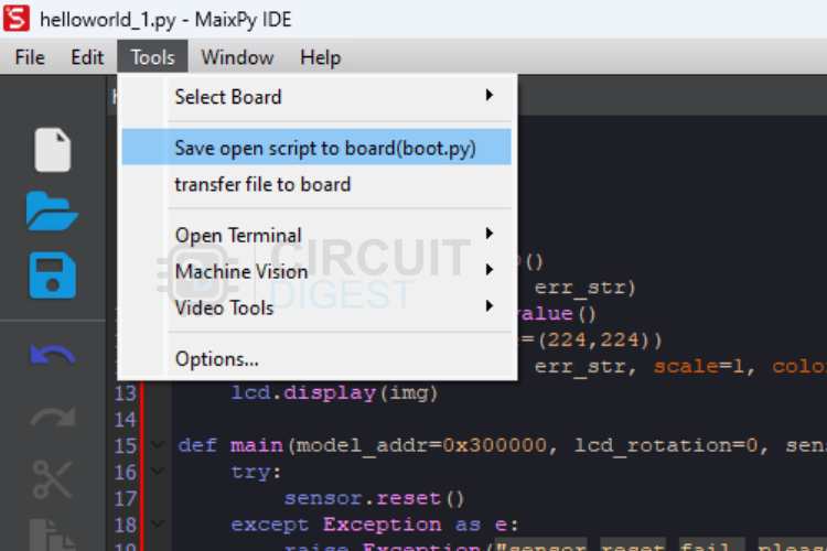
The second method is for when we are using the MaixPy IDE. In the IDE we can choose to save the opened file as boot.py from the tool menu to save the content in the IDE windows as the boot.py file.

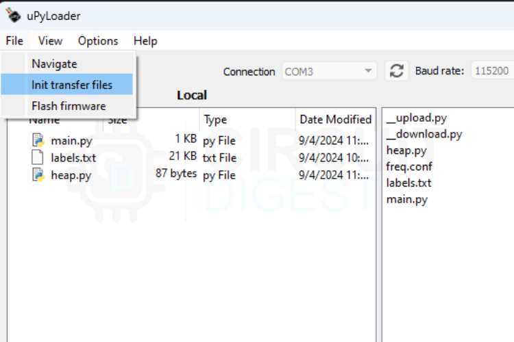
The third method is to use uPyLoader. The uPyLoader gives you an FTP client like user interface where you can add, remove or execute very easily.

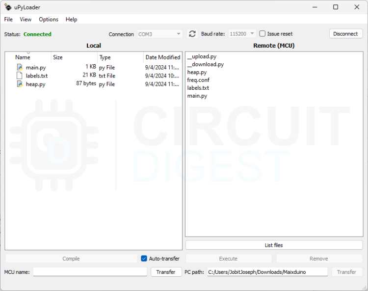
If you face any error when trying to transfer the file for the first time use the Init transfer files from the file menu. 

Executing the Python Scripts

If you want to execute a Python script in the flash memory you can do that in various ways. The first way of course is through the serial terminal. For that first goto the directory where the file is stored using the os.chdir() command, for example, os.chdir("/flash"). Then you can execute the scripts using the import command, for example, import helloworld. This method is simple and easy to use, but it should be noted that the import command can only be used once. If we use the import command for the second time, the file will not be executed again.

Another way is to use the exec() function to execute. Here is a sample code snippet that shows the use of the exec() function.

with open("hello.py") as f:
    exec(f.read())

Another way is to run the program from the MaixPy IDE as we have mentioned before. But with this method, the program is only temporarily running, it will not be saved on the device. You can also execute codes using the uPyLoader. After connecting, select the file and click execute the button to execute the file.

Automatically Running the Code on StartUp

The system will create the boot.py file and main.py in the /flash or /sd (preferred) directory. When booting, it will automatically execute boot.py first, and then main.py (if the SD card is detected, the file in the SD card will be executed). Edit the contents of these two scripts to achieve self-starting. If you write an infinite loop (While True) program in boot.py, main.py will not be able to run. Conventionally, the boot.py is mainly used to configure hardware and only needs to be configured once and the main.py is used for running the main program. So edit those scripts according to your needs.

Board Configuration File

To make the programming much easier we can use the board configuration file. It is nothing but a board definition file with pin mapping for easier understanding. Even though it is not necessary it will help the programming much easier when using the GPIO and onboard peripherals. To use it all you need to do is to run the config_maix_duino.py script once. Which will create a config.json file within the flash and can be used later. Using it is much easier, just import the board_info parameter from the config file and you are good to go. Here is an example where we are turning on the red element of the onboard RGB LED, the pin connected to the red is defined as LED_R in the config file. We can directly use it without checking the schematics for the exact pin number.

from Maix import GPIO
from fpioa_manager import fm
from board import board_info
print(board_info.LED_R)
fm.register(board_info.LED_R, fm.fpioa.GPIO0, force=True)
led_r = GPIO(GPIO.GPIO0, GPIO.OUT)
led_r.value(0)

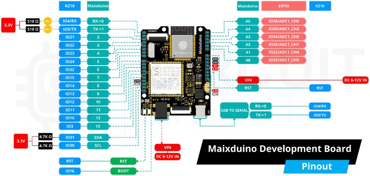
Similarly, all the pins are mapped in a more convenient manner and can easily be used in our code. To know the exact pin mapping you can either open the config_maix_duino.py or the config. You can also refer to the image below, where it shows the Arduino like pin map.

Maixduino MicroPython Bacis

Covering all the basics of Maxduino MicroPython would take multiple articles and nonetheless Sipeed has detailed documentation about that. You may refer the the Sipeed’s Maixduino Specific MaixPy basics documentation for more details about it.

Maixduino AI Neural Network Applications

As we know the main selling points of the K210 AI SoC that is used in the Maixduino are its AI capabilities including Convolutional Neural Network based machine vision and machine learning. So to understand the AI capabilities of the Maixduino board we will look at some AI examples using the pre-trained AI models Sipeed provides.

Face Detection Example

As the name suggests, in this example we will look at the face detection AI model that Sipeed provided. The model will find a face in a picture and frame it and it uses YOLO V2 to detect the faces. To use it make sure to flash the normal or default MaixPy firmware to the Maixduino as instructed in the MaixPy firmware installation section. The next step is to download the pre-trained AI model. For that go to Sipeed’s AI model download page and download the face_model_at_0x300000.kfpkg model file. Once the file is downloaded, download it to the Maixduino’s flash memory using the kflash_gui utility or put it in an SD card. Since reading from the flash memory is always faster than reading from the SD card, it is recommended to load the AI model file to the flash memory, as long as the model file size is within the limit. 

Once it's done we can move forward with the micropython script. You can load the AI model using task = kpu.load(0x300000). In this, the memory address is specified since the model is stored in the flash memory. If you are using the SD card to store the AI model, you can load the AI model into the script using task = kpu.load(0x300000). Then you can set the anchor points as anchor = (1.889, 2.5245, 2.9465, 3.94056, 3.99987, 5.3658, 5.155437, 6.92275, 6.718375, 9.01025). The anchor point parameter is consistent with the model parameter. For each model, this parameter is fixed and bound to the model (determined when the model is trained). It cannot be changed to other values. Later you can initialize the kpu network object using kpu.init_yolo2(task, 0.5, 0.3, 5, anchor). Since this model is used YOLO V2, we used init_yolo2 to initialize the model. This function has a total of five parameters. Those parameters are:

  • kpu_netKPU.load(): kpu network object, that is, the returned value of the loaded model object

  • threshold: Probability threshold. The result will be output only if the probability of this object is greater than this value. The value range is: [0, 1]

  • nms_value: box_iou threshold, in order to prevent the same object from being framed by multiple boxes, when two boxes are framed on the same object, if the ratio of the intersection area of ​​the two boxes to the total area occupied by the two boxes is less than this value, the box with the highest probability is selected.

  • anchor_num: The number of anchor points, fixed here as len(anchors)//2

  • anchor: As mentioned earlier this parameter is fixed and bound to the model

After the initialisation, you can input the image data and run the model as follows.

code = kpu.run_yolo2(task, img)

This will analyse the given image data and will give you the result. Here is a full example code in which the Maixduino will detect the face from the camera feed in real-time and creates a frame on the preview displayed in the LCD display.

import sensor, image, lcd, time
import KPU as kpu
import gc, sys

def lcd_show_except(e):
    import uio
    err_str = uio.StringIO()
    sys.print_exception(e, err_str)
    err_str = err_str.getvalue()
    img = image.Image(size=(224,224))
    img.draw_string(0, 10, err_str, scale=1, color=(0xff,0x00,0x00))
    lcd.display(img)

def main(model_addr=0x300000, lcd_rotation=0, sensor_hmirror=False, sensor_vflip=False):
    try:
        sensor.reset()
    except Exception as e:
        raise Exception("sensor reset fail, please check hardware connection, or hardware damaged! err: {}".format(e))
    sensor.set_pixformat(sensor.RGB565)
    sensor.set_framesize(sensor.QVGA)
    sensor.set_hmirror(sensor_hmirror)
    sensor.set_vflip(sensor_vflip)
    sensor.run(1)

    lcd.init(type=1)
    lcd.rotation(lcd_rotation)
    lcd.clear(lcd.WHITE)

    anchors = (1.889, 2.5245, 2.9465, 3.94056, 3.99987, 5.3658, 5.155437, 6.92275, 6.718375, 9.01025)
    try:
        task = None
        task = kpu.load(model_addr)
        kpu.init_yolo2(task, 0.5, 0.3, 5, anchors) # threshold:[0,1], nms_value: [0, 1]
        while(True):
            img = sensor.snapshot()
            t = time.ticks_ms()
            objects = kpu.run_yolo2(task, img)
            t = time.ticks_ms() - t
            if objects:
                for obj in objects:
                    img.draw_rectangle(obj.rect())
            img.draw_string(0, 200, "t:%dms" %(t), scale=2)
            lcd.display(img)
    except Exception as e:
        raise e
    finally:
        if not task is None:
            kpu.deinit(task)

if __name__ == "__main__":
    try:
        main( model_addr=0x300000, lcd_rotation=0, sensor_hmirror=False, sensor_vflip=False)
        # main(model_addr="/sd/m.kmodel")
    except Exception as e:
        sys.print_exception(e)
        lcd_show_except(e)
    finally:
        gc.collect()

After running this code you can see the result on the LCD display as shown below


You can download the python script for this example from our GitHub Repository. https://github.com/Circuit-Digest/Maixduino-AI-Projects/tree/main/Face%20Detection  

Object Classification Example

For this example, we need to load the minimal firmware to Maixduino since the model itself is a little bigger in size. This model can classify up to 1000 different objects, since the bigger model. After flashing the minimal firmware, download the mobilenet_0x300000.kfpkg model from the download page. Once the file is downloaded, download it to the Maixduino’s flash memory using the kflash_gui utility. Also, download the labels.txt file and save it to the file system. Since the minimum firmware does not support IDE, you can use uPyloader to download the file to the flash. We also need to reduce GC heap size. To do so just run the following script.

from Maix import utils
import machine

utils.gc_heap_size(256*1024)
machine.reset()

Once it's done we can move forward with the main micropython script. Use the following script.

import sensor, image, lcd, time
import KPU as kpu
import gc, sys

def main(labels = None, model_addr="/sd/m.kmodel", lcd_rotation=0, sensor_hmirror=False, sensor_vflip=False):
    gc.collect()

    sensor.reset()
    sensor.set_pixformat(sensor.RGB565)
    sensor.set_framesize(sensor.QVGA)
    sensor.set_windowing((224, 224))
    sensor.set_hmirror(sensor_hmirror)
    sensor.set_vflip(sensor_vflip)
    sensor.run(1)

    lcd.init(type=1)
    lcd.rotation(lcd_rotation)
    lcd.clear(lcd.WHITE)

    if not labels:
        raise Exception("no labels.txt")

    task = kpu.load(model_addr)

    try:
        while(True):
            img = sensor.snapshot()
            t = time.ticks_ms()
            fmap = kpu.forward(task, img)
            t = time.ticks_ms() - t
            plist=fmap[:]
            pmax=max(plist) 
            max_index=plist.index(pmax)
            img.draw_string(0,0, "%.2f\n%s" %(pmax, labels[max_index].strip()), scale=2, color=(255, 0, 0))
            img.draw_string(0, 200, "t:%dms" %(t), scale=2, color=(255, 0, 0))
            lcd.display(img)
    except Exception as e:
        sys.print_exception(e)
    finally:
        kpu.deinit(task)

if __name__ == "__main__":
    try:
        with open("labels.txt") as f:
            labels = f.readlines()
        main(labels=labels, model_addr=0x300000, lcd_rotation=0, sensor_hmirror=False, sensor_vflip=False)
        # main(labels=labels, model_addr="/sd/m.kmodel")
    except Exception as e:
        sys.print_exception(e)
    finally:
        gc.collect()

As you can see, at first we imported all the necessary modules, including sensor, image, LCD and time libraries. Along with that we have also imported the KPU neural network module, garbage collector and system modules. Later you can see the function called main is being declared. This function handles all the image processing and neural network procedures. When the script is run it will first read the labels.txt files is first read and the listed labels from the file is loaded into an identifier called labels. After that the main function is called with five arguments. The first argument points to the labels identifier while the second argument points to the model's memory location. The third argument is to set the display rotation and the fourth and fifth arguments are used to set the horizontal mirror and vertical flip of the camera image.
The main function initialises the camera, display and neural network modules using the provided arguments. After initialisation, the main function will get the image from the camera, run the object identifier model on it and if an object id detected it draws a frame around it and prints the corresponding label. The following line of code is used for object detection.

fmap = kpu.forward(task, img)
plist=fmap[:]
pmax=max(plist)
max_index=plist.index(pmax)

Once the object is detected the result is printed using the following line of code.

img = img.draw_string(0, 0, "%.2f : %s" %(pmax, labels[max_index].strip()), color=(255, 0, 0))
lcd.display(img, oft=(0,0))
print(fps)

As you can see the draw_string function is used to add the label to the image prior to displaying it on the screen. Here is the demonstration of the above script.

You can download the python script for this example from our GitHub Repository. https://github.com/Circuit-Digest/Maixduino-AI-Projects/tree/main/1000%20Object%20Detection 

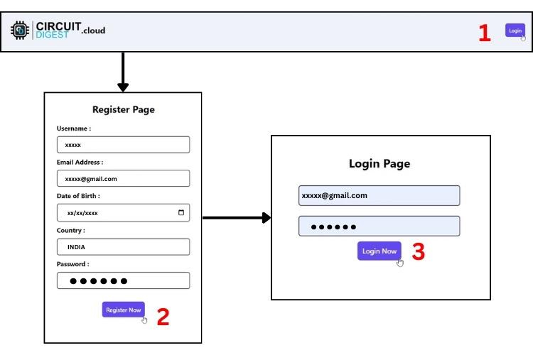
What is MaixHub and how to use it?

Sipeed also has an online platform called Maixhub AI models and training. The Maixhub not only allows you to download pre-trained models but also gives you the option to train your own model. To use it go to the Maixhub page and register a new account, If you are already registered log in to the Maixhub platform.

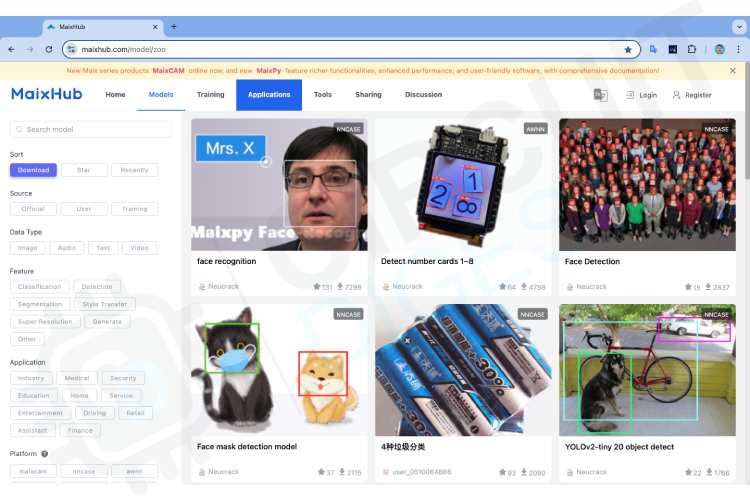
If you click on the Models tab on the top of the page it will redirect you to the page where you can find a ton of pre-trained models to try out. If you want to use them you can open that particular model page and download it. Most of the models would also have the required instructions on the model page itself.

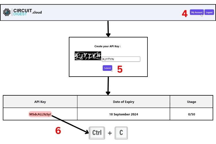
Training Your Own AI Model Using MaixHub

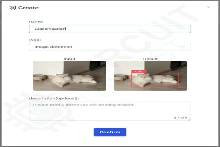
To train sour own AI model first go to the training page on MaixHub.Click on Create to create a new project. Give a project name and select the type, whether it's image classification or image detection. If you just need to identify objects, then select image classification. If you need to identify object categories and output the coordinates of the recognized objects, then choose image detection. It's recommended to train an image detection model first. Image detection training involves dataset annotation, so mastering image detection training means you also master image classification.

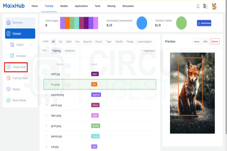
Once the project is created, the next step is to create a dataset. The created dataset can be reused for other projects if needed. Later select the dataset we have created and click confirm.

The next step is to collect training images. We can either upload images, import from datasets, import from device or copy from other datasets. And there is also an option for automatically generate annotated pictures from video.

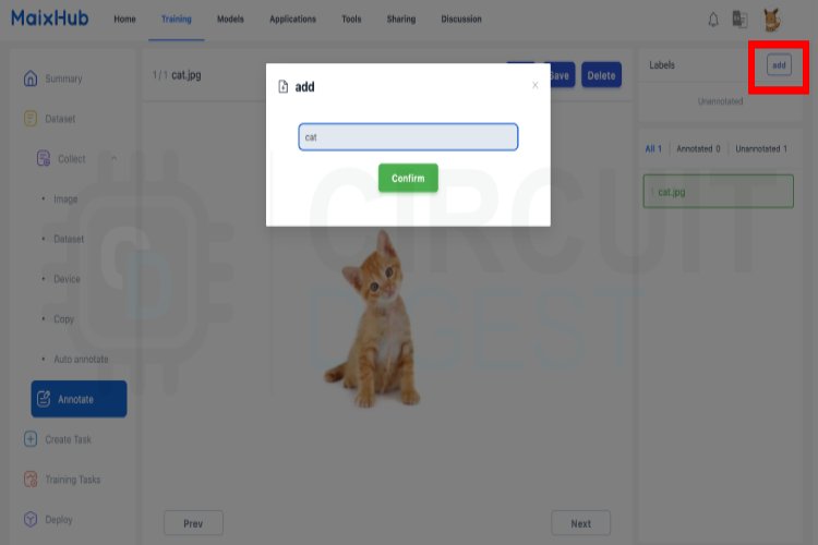
Images uploaded to MaixHub can be annotated within. Select upload images or compressed packages and remember to click start upload.

Once the images are uploaded, we can move forward with annotation. Annotating in MaixHub is very easy. First, create labels, and then click on New button or press w on the keyboard to annotate. Click save or press s for saving the annotation. For annotating the next image either click on next or press d on the keyboard.

Once all the images are annotated, let’s move to the training. For that click on the Create Task from the left panel menu.

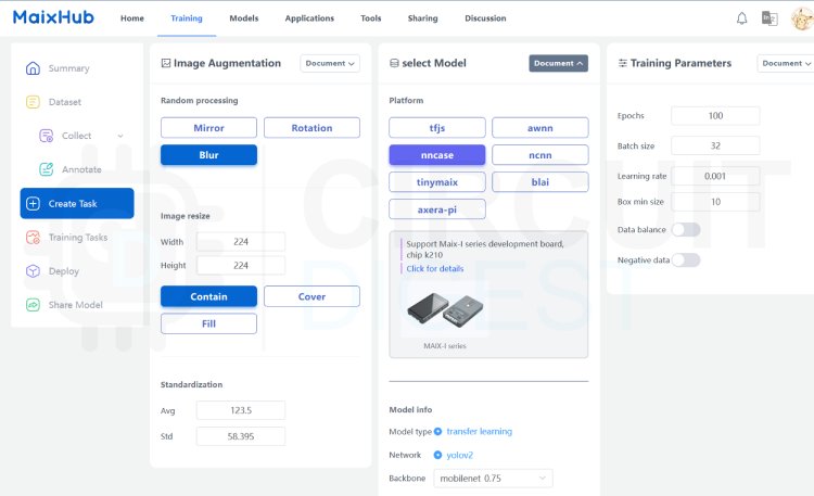
In the task creation page choose the nncase as model for k210, which is the main SoC in the Maixduino, then create a training task and wait for the task to complete.

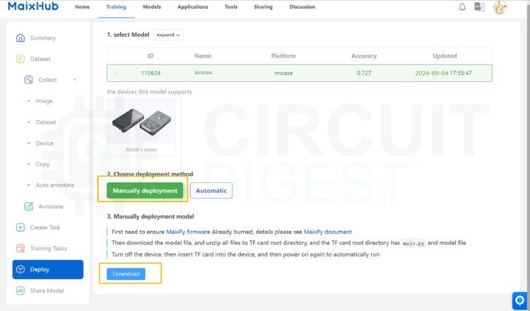
After the model training is completed, click on deploy.In the deployment page choose manual deployment, and click on download to download the model file. The model file with the extension .kmodel will be downloaded to your computer. Use this model on your project.

Now as we gone through the process of using the Maixduino board for Ai projects with MaixPy enjoy creating new projects.

Have any question realated to this Article?

Ask Our Community Members

Brushed or Brushless DC Motor?

Submitted by uploader on

The broad world of DC motors has two basic categories: brushed and brushless. The brushed motor has been around since the 1830s (yes, that long!), and billions of them have been used successfully. However, the brushed motor also has many well-known drawbacks, including brush wear, electrical noise, and controllability issues. Despite these shortcomings, brushed motors have served us well for over 100 years and, for quite some time, were the only DC-powered motor option in many cases.

Several decades ago, the motor situation changed. This was a result of the brushless DC (BLDC) motor, which rose to prominence as electronic commutation was rising in popularity. This popularity was mainly due to two developments: high-energy permanent magnets and low-cost, efficient power-switch devices (MOSFETs and IGBTs) for their coils.

Many larger applications that previously used brushed motors transitioned to brushless designs or variable AC drives (a relative of brushless motors), while smaller motors often shifted to the stepper-motor approach (a close counterpart). Brushed motors appeared to be suitable only for low-cost, low-end, non-critical applications, such as disposable toys, window displays, and similar scenarios where high performance and reliability were not priorities.

Nevertheless, both motor types remain relevant depending on the application, and selecting the right motor size and type can be a challenge. This blog explores the nuanced decision-making process faced when choosing between brushed and brushless DC motors for various applications, considering factors like efficiency, control, and application-specific requirements.

Brushed vs. Brushless Motor Basics

What’s the difference between BLDC and brushed motor arrangements? As seen in the left diagram of Figure 1, the brushed DC motor relies on mechanical commutation to switch the polarity of the magnetic field between the rotor—also known as the armature—and the stator. The stator’s magnetic field is generated by either permanent magnets or electromagnetic coils.

The source current passes through coil windings on the armature. The interaction and constant reversal of the magnetic field between rotor coils and stator induces rotary motion. The commutation action, which reverses the field, is done using physical contacts that are called brushes. These brushes touch contacts on the rotor and bring power to the rotor coils.

The brushed motor can operate directly from the DC rails without any intervening driver or control electronics. This makes it suitable for basic, low-cost, non-critical applications such as simple toys or animated window displays.

In contrast, the brushless motor features an array of electromagnetic coils, called poles, that are fixed around the interior of the housing, with high-strength permanent magnets attached to the rotating shaft (the rotor), as shown in the right diagram of Figure 1. As the poles are energized in sequence by the required control electronics, a process known as electronic commutation (EC), the magnetic field surrounding the rotor rotates and attracts or repels the rotor, which is compelled to follow the field.


Brushed DC vs Brushless DC Motor

Figure 1: A brushed DC motor uses mechanical contacts to implement the commutation and alternating of the magnetic field (left). In contrast, the brushless DC motor design uses electronic commutation and has no wear-prone or EMI-generating moving contacts (right). (Source: Mouser Electronics)

While the current driving the poles can be a square wave, this approach is inefficient and induces vibration, so most designs use a ramping or curved waveform tailored for the desired combination of electrical efficiency and motion precision. Additionally, the controller can fine-tune the energizing waveform for quick yet smooth starts and stops without overshoot, ensuring a sharp response to mechanical load transients. There is a direct and visible relationship between the construction and operation of brushed motors. In fact, brushed motors are so straightforward that they are offered as STEM-focused kits in educational settings (Figure 2).


Classic Brushed DC Motor

Figure 2: A classic brushed DC motor serves as a good teaching and demonstration fixture for electricity, magnetism, and motion basics. (Source: HENADZY/stock.adobe.com)

The Designer’s Tendency

Today’s reality is that when a designer needs a small motor with sub-fractional horsepower for a project, the natural instinct is usually to look at the wide range of standard brushless DC (BLDC) motors first and maybe, just maybe, also consider the brushed motor.

This approach makes sense for several reasons. For one, BLDC motors are easy to drive with modern controller ICs or embedded firmware. Moreover, matching the motor with necessary MOSFET drivers between the processor and motor poles is relatively simple. Lastly, they are reliable and generate minimal EMI due to the absence of sliding-contact brushes.

Therefore, in most cases, when a new product needs a DC motor, the designer’s natural inclination is to think brushless in many cases. However, that would be short-sighted. The reality is that brushed motors are still very viable and have their place in sophisticated designs as well.

Remaining Open-minded

When selecting a DC motor, engineers typically prefer the BDLC motor for most new designs because it has such an attractive combination of benefits and few drawbacks compared to the brushed motor. Designers can choose among many different ratings for voltage, current, torque, and more, while they can also select the needed hardware drivers and control algorithms—in software or embedded in firmware. In addition to basic motor-selection guides, vendors offer application software packages with graphical user interfaces (GUIs), making it easy to set the desired performance attributes such as speed, acceleration/deceleration profiles, and responsiveness.

In contrast, the brushed motor is more difficult to control with precision, and algorithms can only do so much and to a more limited extent. To improve performance, some brushed motor system designs add a rotary-position feedback sensor, such as optical, Hall effect, capacitive, or magnetic. However, this approach adds to the design cost, has mechanical-mounting issues, and increases control complexity. In fairness, while many BLDC installations do not need such a feedback sensor, it is also added in some cases to allow tight closed-loop feedback and more consistent performance.

Still, brushed motors are used for various designs ranging from legacy applications to sophisticated systems, such as automotive functions with well-defined velocity and torque requirements. Many vendors offer driver ICs for BLDC motors and variants suitable for brushed motors. Some vendors even provide automotive-specific, AEC-Q100-qualified brushed motor drivers for that demanding application, which is evidence of their continued viability.

Conclusion

Despite conventional engineering wisdom, brushless is always better for serious applications. In contrast, brushed may be suitable for less critical ones, but the choice between the brushed and brushless DC motor is not necessarily simple. A conscientious engineer will rank project priorities and their relative weight and give a fair look at the various alternatives before deciding which is best in a specific situation.

Have any question realated to this Article?

Ask Our Community Members

Chip Turmoil in US: Ambitious USD 30 Billion Semiconductor Investment Struggles to Show Impact

Submitted by Jerry on

In May 2020, Industry leaders Huang Renxun, Su Zifeng, Tim Cook, Wei Zhejiang, Liu Deyin, and Morris Chang came together in Phoenix, Arizona, to commemorate the opening of TSMC's first plant in the United States. This was considered a crucial event. It was an important turning point in the revival of the US semiconductor manufacturing sector. The world's leading chip manufacturers, TSMC, Intel, and Samsung, were all on board thanks to government subsidies under the CHIPS and Science Act. However, even after four years, the grand vision has yet to materialize.

The United States invested USD 30 billion in the semiconductor sector to restore its industrial glory. However, the effort has encountered significant obstacles rather than a victorious resurgence. Many of the large-scale production projects by TSMC, Intel, and Samsung have been delayed or shelved due to serious difficulties. Approximately 40 percent of these major projects are still inactive. It is now unclear what will happen to the CHIPS Act, which was supposed to be the catalyst for this revival. Deteriorating market conditions intensify the uncertainty, and subsidy regulations are still unclear. As election season draws near, the act's future is in jeopardy and highly vulnerable to unexpected shifts in the political landscape.

The CHIPS Act: High Hopes, Harsh Realities

The CHIPS Act was hailed as a game-changer, promising to bring back America's dominance in semiconductor manufacturing. Leaders in process technology, including Intel, Samsung, and TSMC, received significant subsidies. However, they encountered similar obstacles. Not only did they fail to produce a single chip, but their plans to construct new factories also took longer than anticipated. 

TSMC, for instance, has faced several setbacks. Their Arizona plant, originally set to begin mass production in 2024, is now projected to start in the first half of 2025. The opening of the second wafer facility, initially planned for 2026, has been rescheduled for 2028. There is still uncertainty surrounding the third factory, which was expected to utilize 2nm or more advanced process technologies.

TSMC's Setbacks: What Went Wrong?

The plan seemed simple: build factories, hire local talent, and boost production. But reality has a way of shaking things up. Several factors have contributed to TSMC's challenges in the United States. Firstly, work culture. The company has faced difficulty in hiring local American workers. The American workers find TSMC's working practices unpleasant and harsh. On the other hand, there have been reports of cultural miscommunication, where American workers may have mistreated their Taiwanese colleagues, further complicating the work environment.

These issues have sparked a debate about whether TSMC's U.S. expansion is sustainable in the long run. A significant portion of Taiwanese netizens has expressed concerns, with one even commenting, “Stop forcing TSMC to build factories overseas. The conditions are different. It’s like throwing money into the water or burning it on subsidies?”

Intel and Samsung: Navigating Their Own Set of Challenges

TSMC is not the only company facing challenges. Intel has also encountered delays. Their USD 20 billion Ohio project, which was originally expected to start chip production in 2025, has now been pushed back to 2027-2028. Intel's issues stem from a combination of market constraints and slow government investment in the United States. The root cause of Intel's challenges can be attributed to a combination of market limitations and sluggish government investment in the United States.

Samsung, another semiconductor giant, has faced similar challenges. They have secured a USD 6.4 billion grant from the US and will commence construction of their first wafer fab at the Taylor facility in Texas in 2022. This USD 17 billion project was originally planned to be completed by 2024, with a 4nm process production capability.

Tech Giants Face Challenges in US

The Broader Impact: A Ripple Effect Across Industries

The semiconductor industry isn’t the only sector facing challenges in the U.S. Clean energy technology projects have also been slow to progress. The Chips and Science Act (CHIPS) and the Inflation Reduction Act (IRA), both introduced by U.S. President Joe Biden in August 2022, have not achieved the anticipated success in improving the semiconductor industry in the U.S. In the first year of implementing these measures, a total of 114 projects costing over USD 100 million were announced, with a combined investment totaling USD 227.9 billion.

For example, LG Energy Solutions’ USD 2.3 billion battery energy storage facility in Arizona and Albemarle’s USD 1.3 billion lithium refinery in South Carolina have been shelved. Even the battery component manufacturer Anovion’s $800 million factory in Georgia has faced delays.

In the semiconductor industry, other projects have also been put on hold. U.S. semiconductor manufacturer Pallidus had plans to move its headquarters from New York to South Carolina and open a production line there with a total investment of USD 443 million. The new plant was supposed to be operational by the third quarter of last year, but it has remained idle ever since. Integra Technologies, another U.S. semiconductor company, announced plans last year to invest USD 1.8 billion in building a semiconductor factory in Bel Aire, Kansas. However, uncertainty around government funding has stalled the project.

CHIPS Act Funding in Limbo: What’s Next for U.S. Semiconductor Projects?

As of July 30, 2024, the CHIPS Act Program Office has announced grants and loans totaling over USD 30 billion and over USD 25 billion respectively, according to a report by the Semiconductor Industry Association (SIA). These subsidies have been granted to 14 companies, with the majority going to the five major foundries: Intel, GlobalFoundries, TSMC, Samsung, and Micron. However, the funds have not been distributed yet, despite the announcements. The U.S. Department of Commerce aims to distribute all USD 39 billion in direct incentive grants from the CHIPS Act by the end of 2024. 

The projects, which are expected to exceed USD 284 billion, will have different completion times, with some scheduled for completion by 2025. Other fabs may take anywhere between two to seven years to finish. The SIA suggests that while the CHIPS Act funding could influence the development of some fab sites, it is unlikely to have a significant impact in 2024. Nonetheless, it may lead to increased capital expenditures in 2025.

An Uncertain Political Landscape

In the United States, industries are facing an uncertain future. The political situation is particularly volatile, especially with the upcoming U.S. elections. During his campaign rallies, former President Donald Trump has repeatedly threatened to “repeal the IRA bill on the first day of taking office.” Should Trump return to power, the fate of the IRA and CHIPS Acts could be at risk.

Moreover, unclear subsidy regulations, a declining market environment, and reduced demand have compelled companies to reconsider their strategies. Even with subsidies, the challenges of constructing factories, hiring staff, and sustaining investment remain formidable. President Biden’s policies have sparked numerous inquiries. These policies are designed to generate jobs and economic benefits in the U.S. through industrial transformation.

Conclusion

The U.S. semiconductor industry, along with other tech sectors, is navigating a challenging landscape. Despite significant investments and ambitious plans, the road to success is blurred by delays, cultural clashes, and political uncertainties. The next few years will be crucial in determining whether the U.S. can overcome these hurdles and reclaim its position as a leader in semiconductor manufacturing. For now, the manufacturing environment remains in a state of flux, with no clear answers in sight. But one thing is certain: the journey will continue, with all its twists and turns.

Have any question realated to this Article?

Ask Our Community Members

Number Plate Recognition API for Low-Power Embedded SoC Boards

Today, we are going to take a look at another Circuit Digest cloud API that can perform number plate recognition. Using this Number Plate Recognition API, we can now recognize vehicle license number plates with ease. So, in this article, we will learn about this new Number Plate Recognition API.

Number Plate Recognition API

The Number Plate Recognition API is easy to understand and simple to integrate into various projects. It eliminates the need for complex image processing and machine learning on the user’s end, making it accessible even for microcontrollers with low processing power. By simply capturing an image and sending it to the cloud, the API handles all the backend processing and returns the recognized text. This simplicity allows developers to focus on building their application without worrying about the complicated details of OCR technology. Whether for vehicle identification, security, or automation, this API offers a quick and efficient solution for number plate recognition tasks.

Disclaimer: At the time of writing this article our cloud platform is functional but yet to have some cosmetic updates. We intend to build it with time and add more functionalities

Authentication and Authorization

To use this free Number Plate Recognition API or Any other API Available on circuitdigest.cloud you need to have the API Key. So, let's first Create the API KEY.

Logging in to the Circuit Digest Cloud

Process of Signing into Circuit Digest Cloud Account

Step 1: Visit the Circuit Digest Cloud Home Page. Click the "Login" button located at the top right corner to be redirected to the login page.

Step 2: If you already have an account, log in using your existing credentials. If not, go to the registration page to create an account by filling in the required details. Once completed, click "Register Now" to sign up.

Step 3: After registering, use your email ID and password to log in on the login page.

Generating the API Key

Process of Generating API Key

Step 4: Once logged in, click on "My Account" at the top right corner.

Step 5: You will be directed to a page where you can generate your API Key. Enter the captcha text in the provided box, then click the "Submit" button.

Step 6: If the captcha is correct, you'll see a table displaying your API Key along with its expiration date and usage count. Currently, there is a limit of 50 uses per key. Once you reach this limit, you can generate another key, giving you an additional 50 uses. This usage limit is in place to prevent server overload.

Number Plate Recognition API Details

The API can be easily used with Arduino code snippets to capture a Number Plate image and send it to the server using API for processing. The Server recognizes the Number Plate and returns a response in JSON format. 

Server Name: www.circuitdigest.cloud
Server Path: /readnumberplate
Server Port: 443
Method: POST
Authorization: Authorization: apikey (replace apikey with actual API key)
Content-Type: multipart/form-data; boundary=CircuitDigest
Request Body: The captured image data sent as JPEG file. Filename of image should be same as API key

Response: The server API should return a JSON response containing the decoded information from the Number Plate.

Note: Sample Arduino code for ESP32-CAM and other development boards can be found at the bottom of this page. 

Server API Response

Below is a sample response from the Server API. The top section displays two images: the left image is the raw photo captured by the ESP32-CAM, and the right image shows the result after the recognition process. The bottom section presents the data returned by the API call.

Server API Response

In the image, under the JSON Response, you can find the result in the “number_plate” field, which is “TN 16D1129”.

If you wish to view the uploaded image, you can access it via the link provided in the “view_image” object in the JSON string.

Image Loaded in the JSON Response String

The image above clearly shows the image loaded in the browser using the link from the JSON response string. This link acts as a static storage location, so no matter how many times you upload data, only the most recent data will be stored on the server, and the view link will remain unchanged.

Please note that the recognition process is done for only one number plate at a time. If multiple number plates are present, a random one will be selected for recognition. Additionally, the image should not be completely upside down; a slight tilt is acceptable. Refer to the image below for better understanding.

Valid and Invalid Data Inputs

With all these considerations, please do not judge the API harshly, as it will continue to improve over time. If you have any queries or comments, leave them below. We will respond as soon as possible.

Code Examples

The API has been tested with the ESP32-CAM but can be used with any development boards capable of taking an image and sending it to a web server. We will provide links to all the tutorials using this API, complete with code and circuit diagrams, as usual.

Create and Share:

We hope this will be useful for quickly testing and deploying your ideas. If you build something using the API, please share it with us, and we will mention your work on this page. Happy building!

Have any question realated to this Article?

Ask Our Community Members