How to Select the Best GSM/GPS Module for a Vehicle or Asset Tracking Applications

When starting a project, the first challenge is to select the best parts for it. In the case of a tracking project, the main parts would be the GPS and GSM modules are the main components. This article will help you find the best ones from the choices available in the market. We will discuss the features or specifications you should check before sourcing these parts.

Things to Consider before Purchasing a GPS Module

  • Size: Sizing matters as it may affect not only the size constraints but also other technical parameters like lock time and accuracy etc. For applications like tracking, we will need the module with the smallest size possible without any compromise in the accuracy or the response time, etc.
  • Update Rate: The update rate of a GPS or GNSS module is basically how often it recalculates and reports its position. The standard for most devices is 1Hz (Only once per second). 5-10Hz update rates can be considered if you need them to work on faster vehicles which are not required in most real-life scenarios.
  • Communication Interface: It’s the interface used to communicate with the GPS Module. Serial/TTL or the USB interface is the most commonly used interface type by the GPS module.
  • Communication Speed/Baud Rate Refers to the speed of communication between the microcontroller and the GPS module, in the case of serial interface it is called the baud rate. Higher the baud rate allows for faster GPS data to be sent to the MCU.
  • Navigation Sensitivity dBm figure dictates how prone the GPS module is able to capture the signal from the satellites. Higher dBm indicates that the module is able to better pick up satellite signals
  • Power Requirements include the working voltage and the power consumption. It is necessary to select the proper device because in most cases the modules will be battery powered and we will need to conserve the battery to maximize working time. The average power consumption of most common GPS modules is around 30mA at 3.3V
  • Number of Channels that the GPS module runs will affect your time to first fix (TTFF). Since the module doesn’t know which satellites are in view, the more frequencies/channels it can check at once, the faster a fix will be found. After the module gets a lock or fix, some modules will shut down the extra blocks of channels to save power. If you don’t mind waiting a little longer for a lock, 12 or 14 channels will work just fine for tracking.
  • Accuracy: Lower the distance it can get down to = Higher accuracy. Usually able to find out your location within 30 seconds, down to +/- 10m. Most modules can get it down to +/-3m
  • Antenna: Remember, that little GPS module is receiving signals from satellites about 12,000 miles away in the sky. For the best performance, you want a clear path between the antenna and most of the sky. Weather, clouds, and snowstorms shouldn't affect the signal, but things like trees, buildings, mountains, and the roof over your head, will all create unwanted interference, and your GPS accuracy will suffer. So, the choice of the proper antenna is very crucial.
  • Gain: The gain is the efficiency of the antenna in any given orientation. This applies to both transmitting antennas and receiving antennas.
  • Chipset: The GPS chipset is responsible for doing everything from performing calculations, to providing the analog circuitry for the antenna, to power control, to the user interface. It’s a lot of work, and yet that’s exactly what these tiny GPS units are doing. The chipset is independent of the antenna type, therefore you can have a range of different antennas for GPS modules with specific chipsets. Common chipsets are ublox, SiRF, and SkyTraq, and all contain very powerful processors that allow for fast acquisition times and high reliability. The differences between chipsets usually fall on a balance between power consumption, acquisition times, and accessibility of hardware. So, choosing the best one for our application is a crucial part.
  • Price: Last but not least the price of the module is very important. It is very important to keep everything under the budget.
  • Time to First Fix(TTFF): Time taken for satellite lock after power-up or reboot.

So now as we know what we are looking for in a GPS Module, let us take a look at a few GPS Modules in the market now:

NEO-6M GPS Module

NEO-6M GPS Module

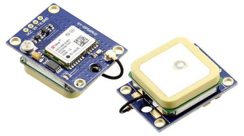
Considered as one of the more popular GPS modules in the market, the NEO-6M module is a family of stand-alone GPS receivers from the NEO-6 module series.

Based on the list of considerations:

Size: 23mm x 30mm

Update Rate: 1 Hz, 5Hz maximum

Power Requirements:

  • Power Supply Voltage: 3V – 5V

Baud Rate: 9600

Communication Interface: UART

Sensitivity: -161dBm

Number of Channels: 50

Time to First Fix:

  • Cold Start: 27s
  • Warm Start: 27s
  • Hot Start: 1s
  • Aided Starts: <3s

Antennas: Includes external patch antenna

Accuracy:

  • 2.5m GPS Horizontal Position Accuracy

Product Applications:

  • Battery-operated mobile devices
  • GPS tracker
  • GPS navigator

NEO-M8N GPS Module

NEO-M8N GPS Module

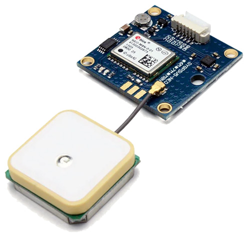
The NEO-M8M GPS Module with Ceramic Active Antenna series of concurrent GNSS modules is built on the high-performing M8 GNSS engine in the industry-proven NEO form factor. The NEO-M8M is optimized for cost-sensitive applications, while NEO-M8N/M8Q provides the best performance and easier RF integration. The NEO-M8N offers high performance also at low power consumption levels. The future-proof NEO-M8N includes an internal Flash that allows future firmware updates. This makes NEO-M8N perfectly suited to industrial and automotive applications.

Based on the list of considerations:

Size: 23mm x 30mm

Update Rate: 1 Hz, 5Hz maximum

Power Requirements:

  • Power Supply Voltage: 3.6V

Baud Rate: 9600

Communication Interface: UART/USB/SPI

Sensitivity: -164dBm

Number of Channels: 72

Time to First Fix:

  • Cold Start: 26s
  • Hot Start: 1s
  • Aided Starts: 4s

Antennas: Includes external patch antenna

Accuracy:

  • 2.5m GPS Horizontal Position Accuracy

Product Applications:

  • Battery-operated mobile devices
  • GPS tracker
  • GPS navigator

SIM28ML

SIM28ML Module

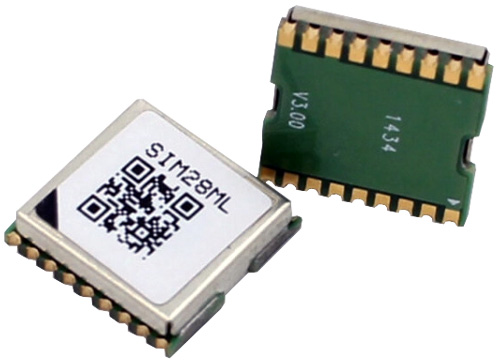
SIM28ML is a small, high-performance, and reliable GPS module. This is a standalone L1 frequency GPS module in an SMT type and it is designed with an MTK high sensitivity navigation engine, which allows you to achieve the industry’s highest levels of sensitivity, accuracy, and Time-to-First-Fix (TTFF) with the lowest power consumption.

Size: 10.1*9.7*2.5mm

Update Rate: Up to 10Hz, 1Hz by default

Power Requirements:

  • Power Supply Voltage: 2.8~4.3V
  • Power consumption
    • Acquisition 17mA
    • Tracking 16mA
    • Backup 8uA

Baud Rate: Adjustable 4800bps~115200bps Default: 9600bps

Communication Interface: UART

Sensitivity: -165dBm

Number of Channels: 22 (Tracking)/ 66 (Acquisition)

Time to First Fix:

  • Cold Start: 32s
  • Warm Start: 3s
  • Hot Start: <1s

Antennas: Embedded patch antenna: 15.0mm × 15.0mm × 4.0mm

Accuracy:

  • 2.5m GPS Horizontal Position Accuracy

Product Applications:

  • Battery-operated mobile devices
  • GPS tracker
  • GPS navigator

Quectel L80

Quectel L80 Module

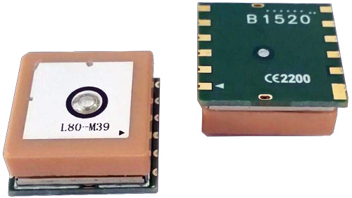
L80 GPS module with an embedded patch antenna and LNA brings the high performance of MTK positioning engine to industrial applications. It is able to achieve the industry’s highest level of sensitivity, accuracy and TTFF with the lowest power consumption in a small-footprint leadless package. With 66 search channels and 22 simultaneous tracking channels, it acquires and tracks satellites in the shortest time even at the indoor signal level. The embedded flash memory provides the capacity for users to store some useful navigation data and allows for future updates.

Size: 16.0mm × 16.0mm × 6.45mm

Update Rate: Up to 10Hz, 1Hz by default

Power Requirements:

  • Power Supply Voltage: 3.0V~4.3V Typical voltage: 3.3V

Baud Rate: Adjustable 4800bps~115200bps Default: 9600bps

Communication Interface: UART

Sensitivity: -165dBm

Number of Channels: 22 (Tracking)/ 66 (Acquisition)

Time to First Fix:

  • Cold Start: 35s
  • Warm Start: 30s
  • Hot Start: 1s

Antennas: Embedded patch antenna: 15.0mm × 15.0mm × 4.0mm

Accuracy:

  • 2.5m GPS Horizontal Position Accuracy

Product Applications:

  • Battery-operated mobile devices
  • GPS tracker
  • GPS navigator

Beitian BN-220

Beitian BN-220 Module

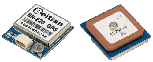
BN-220 is a small gps receiver module, with 4M flash to save the configuration. It is mostly used with drones.

Size: 16.0mm × 16.0mm × 6.45mm

Update Rate: 1Hz-10Hz,Default1Hz

Power Requirements:

  • Power Supply Voltage: 3.0V~5.5V Typical voltage: 5V

Baud Rate: Adjustable 4800bps~921600bps Default: 9600bps

Communication Interface: UART

Interface Protocol: NMEA-0183orUBX,DefaultNMEA-0183

Sensitivity: -167dBm

Number of Channels: 72Channel(Acquisition)

Time to First Fix:

  • Cold Start: 26s
  • Warm Start: 25s
  • Hot Start: 1s

Antennas: Embedded patch antenna

Accuracy:

  • 2m GPS Horizontal Position Accuracy

Product Applications:

  • Drones

Grove – GPS Module

Grove – GPS Module

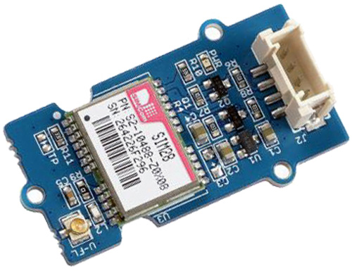
The Grove – GPS Module is the Seeed version of a GPS receiver that’s cost-efficient and field-programmable. It’s armed with a SIM28 and serial communication configuration.

Size: 40mm x 20mm x 13mm

Update Rate: 1 Hz, max 10 Hz

Power Requirements: 3.3/5V

Baud Rate: 9600 – 115,200

Communication Interface: UART

Sensitivity: -160dBm

Number of Channels: 22 tracking/66 acquisition channels

Time to First Fix:

  • Cold starts with EASY: 13s
  • Warm Starts with EASY: 1-2s
  • Hot Starts: <1s

*EASY is a self-generate orbit protection

Antennas: Antenna included in the package

Accuracy: 2.5m GPS Horizontal Position Accuracy

Product Applications:

  • GPS tracker
  • GPS navigation
  • Distance measurement

Other Product Features:

  • Low power consumption
  • Baud rates configurable
  • Grove compatible interface

Grove – GPS (Air530)

Grove GPS Air530

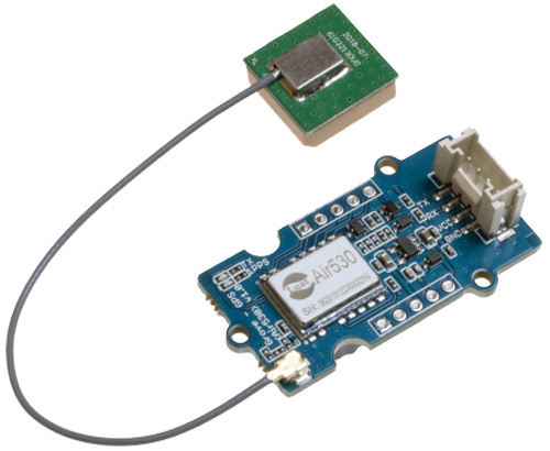
Next up, we have the Grove – GPS (Air530). It’s a high-performance, highly integrated multi-mode satellite positioning and navigation module. It supports GPS / Beidou / Glonass / Galileo / QZSS / SBAS, which makes it suitable for GNSS positioning applications such as car navigation, smart wear, and drone.

If your GPS isn’t working well in urban areas or outdoors under only one or a few satellite modules, you should definitely check out this GPS module. Meanwhile, this module is capable of receiving more than 6 satellites at the same time and is able to work excellently even if there’s a very bad signal.

This GPS adopts the integrated design of RF baseband, which integrates DC/DC, LDO, LNA, RF front-end, baseband processing, 32-bit RISC based chip, RAM, FLASH storage, RTC and power management functions.

Size: 40mm x 20mm x 13mm

Update Rate:

Power Requirements: 3.3/5V

Baud Rate: – 9600 –921600

Communication Interface: UART

Sensitivity: – –166dBm

Number of Channels:

Time to First Fix:

  • Cold start: 30 seconds
  • Warm Start: 4 seconds

Antennas: Antenna included in the package

Accuracy: 2.5m Horizontal positioning accuracy

Product Applications:

  • GPS tracker
  • GPS navigation
  • Distance measurement

Other Product Features:

  • Highly integrated Multi-mode satellite positioning and navigation
  • Grove compatible interface

Things to Consider before Purchasing a GSM Module

  • Size: Similar to the GPS module the size matters in the case of a GSM module too. The smaller the size more compact our project will be.
  • Communication Interface: It’s the interface used to communicate with the GSM Module. Serial/TTL or the USB interface is the most commonly used interface type by the GSM module.
  • Communication Protocol: Communication protocol is used to communicate with the module. Most modules use AT Commands for this purpose. With AT commands, there will be commands to control each function of the module. We will use these commands to configure the module, to get information from the module, for services SMS, MMS and for voice and data links too.
  • Communication Speed /Baud rate Refers to the speed of communication between the microcontroller and the GSM module, in the case of serial interface it is called the baud rate. Higher the baud rate allows for faster GSM data to be sent to the MCU.
  • Communication Standard refers to the mobile standards like GSM, CDMA, WCDMA, LTE etc. GSM commonly stands for 2G, WCDMA for 3G and LTE for 4G communications. And the CDMA is no longer used in most areas of the world.
  • Supported Frequency Bands refers to the frequency bands supported by the module. 900MHz and 1800Mhz are the most common 2G bands in India while 900MHz and 2100MHz are the 3G bands. And for 4G the most common bands used in India are  B1 (2100 MHz), B3 (1800 MHz), B5 (850 MHz), B8 (900 MHz), B40 (TDD 2300 MHz), B41 (TDD 2500 MHz). So it is very important to choose the correct module which supports the bands supported by the carrier in the intended area.
  • Supported services refers to the services supported by the module including voice, SMS and data. Some even support FM. Not all modules support all the protocols. So be careful when choosing the correct one.
  • Data Transmission Throughout It refers to the maximum upload and download data speed supported by the module. For example, the most famous SIM800L has a maximum upload and download speed of 85.6kbps, while the SIM7500 module supports up to 150Mbps of download and 150Mbps of upload speed in LTE Category 4. So, if our applications need more bandwidth we must choose accordingly.
  • Transmit Power: Transmission power of the module. Higher the power higher the reception, but with higher power usage. Not only that the power regulation may vary with countries so make sure to choose the correct module with proper transmission power rating as per your regulatory authorities.
  • Power Requirements: This includes the working voltage and the power consumption. It is necessary to select the proper device because in most cases we will the modules will be battery powered and we will need to conserve the battery to the maximum.
  • Price: Last but not least the price of the module is very important. It is very important to keep everything under the budget.

So now as we know what we are looking for in a GSM Module, let us take a look at a few GSM Modules in the market now:
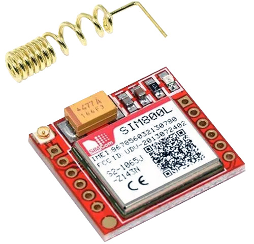
SIMCOM SIM800L

SIMCOM SIM800L

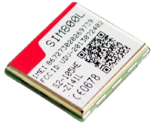
SIM800L is a quad-band GSM/GPRS module, that works on frequencies GSM850MHz, EGSM900MHz, DCS1800MHz and PCS1900MHz. SIM800L features GPRS multi-slot class 12/ class 10 (optional) and supports the GPRS coding schemes CS-1, CS-2, CS-3 and CS-4. With a tiny configuration of 15.8*17.8*2.4mm, SIM800L can meet almost all the space requirements in user applications, such as smartphones, PDA and other mobile devices. SIM800L has 88pin pads of LGA package and provides all hardware interfaces between the module and customers’ boards.

SIM800L GSM Module

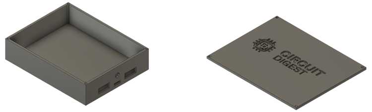
It is also available as a module. The image of the module is given above.

Size:  15.8*17.8*2.4mm

Communication Interface:  UART/USB

Communication Protocol: AT Command

Communication Speed /Baud rate: 1200bps to 115200bps

Communication Standard: GSM GPRS(2G)

Supported Frequency Bands: Quad-band: GSM 850, EGSM 900, DCS 1800, PCS 1900

Supported services: Voice, SMS, DATA GPRS

Data Transmission Throughout: GPRS data downlink transfer: max. 85.6 kbps/GPRS data uplink transfer: max. 85.6 kbps 

Transmit Power: Class 4 (2W) at GSM 850 and EGSM 900, Class 1 (1W) at DCS 1800 and PCS 1900

Power Supply: 3.4V ~4.4V typical power consumption in sleep mode is 0.7mA

Ai Thinker A9 GPRS Series Module

​Ai Thinker A9 GPRS Series Module

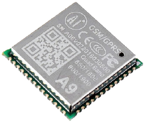
Ai Thinker A9 GPRS Series Module can be used in a wide range of IoT applications and is ideal for IoT applications for home automation, industrial wireless control, wearable electronics, wireless location sensing devices, wireless location system signals, and other IoT applications. The A9 is a complete quad-band GSM / GPRS module in a compact design SMD package. Its stable performance, appearance of compact, and cost-effective, could meet the diverse needs of customers.

Size: 19.2*18.8*2.7mm

Communication Interface: UART/USB/I2C

Communication Protocol: AT Command

Communication Speed /Baud rate: 1200bps to 115200bps

Communication Standard: GSM GPRS(2G)

Supported Frequency Bands: 850, 900, 1800, 1900MHZ

Supported services: Voice, SMS, DATA GPRS

Data Transmission Throughout: GPRS data downlink transfer: max. 85.6 kbps/GPRS data uplink transfer: max. 42.8Kbps

Transmit Power: Class 4 (2W) at GSM 850 and EGSM 900, Class 1 (1W) at DCS 1800 and PCS 1900

Power Supply: 3.8V-4.2V, 4V power supply is recommended

IoT-GA6 Mini GPRS GSM Module

IoT-GA6 Mini GPRS GSM Module

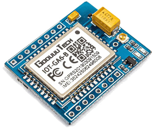
GA6 module is a mini version of serial GSM / GPRS core development board based on GPRS A6 chip. This chip supports GSM/GPRS network, available for GPRS and SMS message data remote transmission. With the help of the A6 chip, GPRS never deactivated until its application is on and online. It supports either digital and analog audio, with HR, FR, EFR, AMR voice coding. This module can add voice, text, SMS, and data capabilities to your Arduino project. It has more price to performance value than the SIM800, SIM900 modules. This small and low power consumption module can communicate with the microcontrollers and Arduino boards through the UART interface, with the capability of command reception, including GSM 07.07, GSM 07.05 standards. It can be used for IoT projects, M2M applications, industrial automation, BMS projects, home automation, public transportation, personal tracking, electricity environment detection, wireless POS, smart metering, and other M2M applications

Size: 17.6*15.7*2.3mm

Communication Interface: UART/USB

Communication Protocol: AT Command

Communication Speed /Baud rate: 115200bps

Communication Standard: GSM GPRS(2G)

Supported Frequency Bands: Quad-band: GSM 850, EGSM 900, DCS 1800, PCS 1900

Supported services: Voice, SMS, DATA GPRS

Data Transmission Throughout: GPRS data downlink transfer: max. 85.6 kbps/GPRS data uplink transfer: max. 42.8kbps 

Transmit Power: Class 4 (2W) at GSM 850 and EGSM 900, Class 1 (1W) at DCS 1800 and PCS 1900

Power Supply: 3.5V ~ 4.2V 3.3V Logic

Quectel M66

Quectel M66 GSM Module

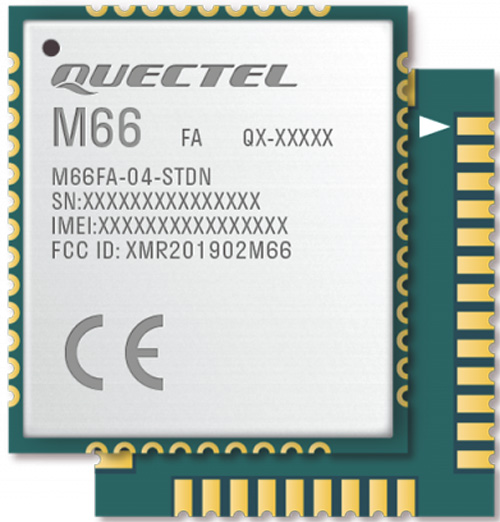
The M66 is a quad-band GSM/GPRS 2G module measuring 17.7mm × 15.8mm × 2.3mm which uses LCC castellation packaging. Based on the latest 2G chipset, it is optimized for data, SMS and audio transmission, and is designed for low-power IoT use cases that operate in harsh conditions. The M66 uses surface-mounted technology, making it ideal for large-scale manufacturing, which can have strict requirements on cost and efficiency. The M66’s ultra-compact profile makes it particularly suited to size-sensitive applications, and the module can serve a range of applications such as wearable devices, automotive, PDAs, asset tracking, POS, smart metering and telematics.

Size: 17.7mm × 15.8mm × 2.3mm

Communication Interface: UART/USB

Communication Protocol: AT Command

Communication Speed /Baud rate: 115200bps

Communication Standard: GSM GPRS(2G), Bluetooth 3.0

Supported Frequency Bands: Quad-band: GSM 850, EGSM 900, DCS 1800, PCS 1900

Supported services: Voice, SMS, DATA GPRS

Data Transmission Throughout: GPRS data downlink transfer: max. 85.6kbps/GPRS data uplink transfer: max. 85.6kbps 

Transmit Power: Class 4 (2W) at GSM 850 and EGSM 900, Class 1 (1W) at DCS 1800 and PCS 1900

Power Supply: 3.3V ~ 4.6V

SIMCOM SIM868

SIMCOM SIM868 Module

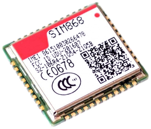
SIM868 module is the complete Quad-Band GSM/GPRS module which combines GNSS( GPS/GLONASS/BDS) technology for satellite navigation. It has strong extension capability with abundant interfaces including UART, USB2.0, GPIO etc. The module provides much flexibility and ease of integration for customers’ applications.

Size: 17.6*15.7*2.3mm

Communication Interface: UART/USB

Communication Protocol: AT Command

Communication Speed /Baud rate: 1200bps to 115200bps

Communication Standard: GSM GPRS(2G)

Supported Frequency Bands: Quad-band: GSM 850, EGSM 900, DCS 1800, PCS 1900

Supported services: Voice, SMS, DATA GPRS

Data Transmission Throughout: GPRS data downlink transfer: max. 85.6 kbps/GPRS data uplink transfer: max. 85.6 kbps 

Transmit Power: Class 4 (2W) at GSM 850 and EGSM 900, Class 1 (1W) at DCS 1800 and PCS 1900

Power Supply: 3.4V ~ 4.4V

Update Rate: Up to 10Hz, 1Hz by default

Power Requirements:

  • Power Supply Voltage: 3.0V~4.3V Typical voltage: 3.3VCommunication Interface: UART

Sensitivity: -167dBm

Number of Channels: 33 tracking /99 acquisition

Time to First Fix:

  • Cold Start: 28s
  • Warm Start: 22s
  • Hot Start: 1s

Antennas: External

Accuracy:

  • 2.5m GPS Horizontal Position Accuracy

Conclusion

We are concluding this article hoping you got a better idea about the available option for a GPS/GSM module. In the article, we haven’t included any 3G/4G modules since they are not good for such an application, and they are very costly at this point. 2G GSM modules will give the best result because of their coverage and they are dirt cheap nowadays. And modules we have covered are the most common available once in the market and many other variants are there too. You may extend your scope to them if you can’t find a suitable one from the above suggestions.

Have any question realated to this Article?

Ask Our Community Members

DC to DC Converter with Constant Current (CC) and Constant Voltage (CV) Control - Schematics, PCB, Parts List, and Working

In this article we will be learning about the features and working of the XL4015 which is a 5A 180KHz 36V Buck DC to DC Converter. Here we will desolder all the components from the module, completely reverse engineer the schematic and make the PCB from it, so that we can order the components and make the PCB ourselves. In addition, we'll test the module and compare all the datasheet parameters to see if they hold true or not. So without further ado let's get right into it.

XL4015 DC-DC Buck Converter Module Features

A Constant Current (CC), and Constant Voltage (CV) converter can come in very handy in various conditions, for example, if you want to charge a lithium battery with a constant current you can do that very easily with this module. Furthermore, if you are testing a circuit and powering it for the first time it's always recommended to use a constant current that will limit damage to your circuit if you made any mistakes in the build process.

XL4015 DC DC Buck Converter Module

In the above image you can see first we have the DC input connector, which is to connect to an unregulated power source. Next, we have two 10K potentiometers that are used to set the constant current and voltage level. Furthermore, there are three LED indicators on the board; the first one near the input connector shows when the module is in constant current mode, while the other two near the output are mainly for battery charging applications (battery charging and battery full indicators). Other than that, this IC has an input voltage range of 8V to 36V, and the output voltage of the device is 1.25V to 32V. With max load, the PWM of the device can reach 100% duty cycle and it can operate on a 180 kHz operating frequency. The constant output current of the module is 5A and it can reach up to 96% efficiency while working. If we are talking about protection features it has thermal shutdown, short circuit protection, and current limit functionality.

Components used in DC-DC Buck Converter

Before we look at the schematic, here is a list of components that are required to build the XL4015 Buck Converter Circuit. The main component in this board is the XL4015 buck converter IC, that is a 5pin IC designed and developed by XLSEMI which is a well-known manufacturer in china and very famous for producing compact buck and boost converter ICs. The list of components required to build the 5A Buck Converter Circuit is shown below-

DC DC Buck Converter Components

  • XL4015 Buck Converter IC - 1
  • 78L05 Voltage Regulator - 1
  • LM358 op-amp - 1
  • SS54 Schottky Diode- 1
  • TL431 Programmable Reference - 1
  • 470uF,35V Capacitor - 2
  • 10uF 0805 Capacitor -2
  • 10K Ten Turns Trim Pot - 2
  • 0.1uF Capacitor - 3
  • 270R Resistor - 1
  • 1K Resistor - 2
  • 2.2K Resistor - 1
  • 10K Resistor -  1
  • 71.5K Resistor - 1
  • 90.9K Resistor - 1
  • LED 0805 - 3
  • Screw Terminal - 2

Circuit Diagram of the XL4015 5A Buck Converter

The Schematic of the Buck converter is shown below. As you can see it's not that difficult to understand and the overall design of the module is indeed a pretty neat and clever piece of work. The schematic diagram of the module is shown below.

XL4015 DC-DC Buck Converter Schematic

The working of the circuit is simple and difficult at the same time. If we check the datasheet of the XL4015 5A buck converter Module, we can see the typical application schematic that is given below.

XL4015 Module Application Schematic

Now compare the above schematic to our schematic, you can see that it's very similar because the schematic for the buck regulator portion stays the same the only additional difference is that it has additional current limiting functionality.

Now let's understand how the current limiting functionality works. In the schematic, you can see we have a 78L05 Voltage Regulator which is an ultra-low-power regulator that is used to convert the input voltage to a constant 5V for the TL431 IC. The TL431 is a reference that is set to a constant current regulator mode with the help of a 71.5K resistor and a potentiometer. This reference is compared to the sense voltage from the output side of the resistor to limit the current. The circuit shown below is the TL431 circuit that is providing a constant current source to the op-amps. 

TL431 Circuit

Next, we have the first op-amp portion; this portion of the circuit is actually used to limit the current. What happens in this portion is that the output sense voltage gets compared with the reference voltage from the TL431 IC. Next what happens is that if the output sense voltage is greater than the reference voltage the output of the op-amp turns high and with the shutdown function of the circuit, the output of the IC turns off.

Buck Converter Schematic

In the above image, I have shown you an application circuit from the datasheet with a practical circuit side by side. So in the practical circuit, the manufacturer uses an LED instead of a diode, this LED not only acts as a reverse current blocking but also lights up when the current limit function is active.

Buck Converter Module Circuit

Next, we have the final portion of the circuit, this portion of the circuit is used to indicate the battery charging and fully charged condition. In this circuit when the battery is fully charged, the output goes low so the charging complete LED turns on, now if a battery is charging, the other LED turns on to indicate the battery is charging.

Recreating the PCB for XL4015 Buck Converter

As we have already made the schematic we thought to recreate the PCB for the buck converter modules and we did just that. The dimension of the PCB is 25mm / 50mm. You can see that from the image below.

XL4015 Buck Converter Module PCB Design

Next, we have used the Manufacturing functionality of eagle to determine the top and bottom portion of the PCB and it looks like something that is shown below.

XL4015 Module PCB

In the above image, the TOP side of the PCB is shown, and the bottom side of the PCB is shown below-

XL4015 Buck Converter PCB

That's all for the PCB part and you can download the Gerber file for the project by clicking the given download link.

Testing the XL4015 DC-DC Buck Converter Module

To start the test, we first connect the buck converter module to the power supply and connect the output to the DC load, and we have set a constant load of 1A to test the circuit.

XL4015 Buck Converter Working

Now as that was working, we set the constant current to 5A as it was advertised in the datasheet.

XL4015 CC CV Module Working

If you consider the size of the module I was very impressed to see that it was able to deliver, a constant current of 5A. I tested this circuit for 5 minutes and it was working absolutely fine.

DIY DC DC Buck Converter Module

Next, we tested this circuit for short circuit conditions. As advertised on the datasheet it has built-in short circuit protection, so we also tested that. And it worked absolutely fine.

Problems Encountered while testing the Buck Converter Circuit

While testing the circuit we encountered a major problem in some of these modules. At the time of writing the article, we had 10 modules in our lab but some of those were working, and some of those were not. This made us very confused.

DC DC Buck Converter Module Problem

But the solution to this problem was very simple: we connected a 1uF capacitor to the PCB and the module worked absolutely well without any issues. Other than that we did not find any problems with the module board.

Conclusion

I tested the module under various input/output voltages and load conditions and evaluated its efficiency, and all the tests went smoothly without any issues. So we can say that the XL4051 is a very cost-efficient and highly effective module for demo projects and battery charging.

Have any question realated to this Article?

Ask Our Community Members

How will 5G Support and Benefit India’s Upcoming Technologies and Applications?

A year back, the government of India has taken an initiative to craft the country into a five trillion dollar economy towards the end of 2025, and one of the key requirements to turn this goal into a reality is revolutionizing the nation’s digital infrastructure. The country has already dug deep into enhancing the digital infrastructure, but experts claim that 5G services will be the key to a successful digital India. The question still remains when will 5G be available in the country in a full-fledged way. To answer this question, the Department of Telecommunications (DoT) recently stated that it will be available in mid or Q4 of 2022. The department also proclaimed that at first the services will be available in 13 cities and then the rest of the country will enjoy the benefits of this service. Ahmedabad, Bengaluru, Chandigarh, Gandhinagar, Gurugram, Hyderabad, Jamnagar, Kolkata, Chennai, Lucknow, Pune, Delhi, and Mumbai are the first 13 cities to enjoy 5G.

5G has ultra-low latency through which it will offer speedier and seamless communication all over the world. This next-generation cellular technology will spearhead and empower modern cutting-edge technologies such as the Internet of Things (IoT), Artificial Intelligence (AI), Augmented Reality (AR), Virtual Reality (VR), and machine-to-machine communications. It will ultimately support a huge range of modern applications and use cases such as self-driving, facial recognition systems, connected devices, chatbots, and many more. In an interaction with the media, Nitin Bansal, managing director of Ericsson India said 5G will boost the economic growth in India and it will assist service providers in monitoring and managing the increasing data requirements of consumers in an efficient manner. The early use-cases for 5G in the country are speculated to be fixed wireless access (FWA) and enhanced mobile broadband (eMBB) that would aid in solving the troubles of limited fixed broadband services and perk up the data experience while on the go.

Now, the question is why India needs 5G badly in 2022. Satyajit Sinha, Senior Analyst at IoT Analytics told CircuitDigest, "The mobile operators will not only be assisted by 5G in monitoring the escalating data requirements of consumers, but also open the gates of revenues for them. 5G is already perking-up various industries in the world via commencing the fourth industrial revolution and by improving the network experience for several businesses and end consumers. In fact, 5G is speculated to spearhead the digital transformation of several sectors like education, energy and utilities, automotive, healthcare, manufacturing, and many more. Towards the end of 2030, the anticipated worth of 5G-enabled digitalization revenues in the country will reach around USD 17 billion.”

5G IoT Applications

Source: Pixabay

How 5G will Lead India’s Digital Transformation by 2025

People in the remote corners of the country enjoyed the benefits of 4G in a better way, but at the same time, we cannot overlook the imperativeness of broadband connectivity for the financial and social enhancement of the nation. The lockdowns have underlined the significance of connectivity in every aspect of our life starting from introducing work from home, the commencement of online trade on a large scale, online education and most importantly, connecting people. The digital India initiative that centers on empowerment depends massively on connectivity and the mobile networks in the country continue to offer its services on that promise.

According to telecom experts, 5G is not only about some giga-bit data speeds. In the beginning, the fuss was about the speed of the 5G deployments, but it is going to transform our life the way we live and play, and work. The fundamental shift from 4G to 5G would be multi-dimensional and the immensity is much bigger than the shift from 3G to 4G. 5G will not only offer a wide range of new-fangled spectrum to be put to use, but it will also become more effective than 4G in the spectrum already in utilization. It can accumulate more data than 4G for the same volume of spectrum.

5G will fetch a huge transformational shift in the teaching domain with remote learning coupled with teaching in the classroom to intelligently escalate the educational efficacies. In India, where 70 percent of people live in rural areas it becomes too difficult to provide top-notch education to everyone manually. Hence, 5G backed by ultra-low latency and higher speed will provide proper education and cater to a wider population. Then, when it comes to smart cities and smart homes, devices furnished with sensors communicating to each other will turn into key equipment. For homes specifically, people might witness cutting-edge AI backed personalization, automated grocery lists, tracking electronic devices, and automated deployment of everyday routines. In terms of smart cities, 5G has the potential to offer smart metering systems and smart electricity grids, safety mechanisms, waste disposal systems, and smart traffic management.

Highlighting the importance of 5G in India’s digital transformation, Lt. Gen Dr. S.P Kochhar, Director General, Cellular Operators Association of India (COAI) said, "With the Prime Minister’s inauguration of the 5G testbeds, the industry is on the pathway towards indigenization of 5G and it opens up opportunities for various other new-age technologies such as big data analytics, artificial intelligence (AI), augmented reality (AR) and virtual reality (VR), etc. which will drive major innovations across industries – Manufacturing, Supply Chain, Healthcare, Transportation and bring us closer towards our vision i.e. Digital India. A couple of impediments like cutting-edge infrastructure and Right of Way (RoW) policies being discussed thoroughly among the regulatory bodies and the unveiling of Gati Shakti Sanchar Portal is yet another promising move for the Indian telecom industry. Industry associations like COAI are working closely with the regulatory bodies and service providers to navigate through the challenges and further amplify the initiatives launched by the Government of India.”

COAI also added that 5G network rollout is expected to add $450 billion to the Indian economy, increasing the pace of development and creating jobs. Prime Minister Narendra Modi recently said that 5G technology will bring positive change in the governance of the country, ease of living, and ease of doing business, especially newer opportunities for the B2B businesses.

Current Role of 5G in Averting Security Risks for IoT Devices

In the coming few years, the volume of IoT connections is expected to augment all over the world, which is about 25.2 billion towards the end of 2025, predicts GSMA Intelligence unit. The report also highlighted that over 3.1 billion out of the 25.2 billion would employ cellular technologies comprising low power wide area Mobile IoT networks. These days, a lot IoT backed devices utilizes wireless technology that comprises of short-range technologies, mostly utilizing unlicensed spectrum such as ZigBee, WiFi, and Z-Wave, and also and wide area cellular technologies, using licensed spectrum, such as LTE, 5G, and GSM. According to experts, cellular technologies that operate under a licensed spectrum offer a huge number of advantages for devices powered by IoT. These are mostly service enablement, sophisticated provisioning, and also device management. Apart from that cellular networks provide a huge international coverage and accurate reliability, performance, and security, which are required by the most promising and in demand IoT applications.

Now, talking from a security perspective, there could be 1.8 billion 5G connections by the end of 2025 as per the GSM association. Back in 2020, the 5G IoT market reached a value of USD 1.5 billion and is speculated to stand USD 40 billion by the end of 2026, at a CAGR of 72.9 percent over the time slot between 2021-2026. When 5G is amalgamated with IoT, it escalates the operational performance of several devices, but at the same time, high-end risks emerge. According to Satyajit Sinha, there is huge difference between deployment of IoT and deployment of 5G, which is regarding the standards that are available in either of these technologies.

5G IoT Module Forecast B2B Market

Basically, the IoT powered devices are still highly unregulated and then follow no generic standards. An IoT device is crafted out of hardware and sensors that further connect a layer of software and the sensors. The software manages the hardware and sensor data and also does the computing. Apart from that, there is a communication interface available that permits connection to the 5G network. Now, crafting a basic security architecture is highly intricate as there are several ways to design, build, and utilize an IoT product.

The current risk assessments and methods are not perfectly designed to get to know about the IoT-based risks in a comprehensible manner. The devices will be on all the time and will be connected to the 5G network and ubiquitous. For instance, if you carefully look at smart home implementation, if there is a voice-enabled device, which is connected to an IoT-powered lock on the door, the person opens the door with his or her voice command. It is not fully secured because a thief who came to know the person has left the home, can come to the door and speak with the same voice command and can open the door. The point is there is absence of authentication at the IoT device. Now, another point to be noted is that 5G will still suffer from the 4G weakness, claims experts. Now, it is not possible to unleash a comprehensive 5G network all at once and in fact, in fewer places 5G is moderately deployed side by side a 4G software components and hardware for a certain time slot. Hence, to have a sturdy IoT security platform or a framework, it requires a multi-layered approach.

Conclusion

5G, after a constant transformation in the last two years, has grown from an emerging idea into a pervasive and important technology for mobile devices. The features of 5G that includes ultra-high density, ultra-high-speed, and ultra-low latency will be inserted into AI via wireless. The AI actions can be completed rapidly through 5G on the terminal side and it also perk-up personalized services, boost customer experience and decrease latency. In fact, 5G will also be benefited from the AI-enabled processing ability.

Highlighting the advantages, Neil Shah, Research Vice President at Counterpoint Research said, “The applications that are based on AI can respond in the accurate time to the data generated by the 5G networks, thereby offering new-fangled potentials for automation. Removing the conventional wireless algorithms with the help of proper machine learning, AI will be able to significantly decrease the price of manpower and enhance the total performance. It will also offer safety to the people’s everyday life, encouraging digital transformation, modernizing several commercial and industrial activities, and unleashing endless top-notch products and services.”

Have any question realated to this Article?

Ask Our Community Members

Raspberry Pi Pico Variants – A Detailed Comparison

Raspberry Pi Pico is a low-cost, versatile microcontroller development board from the Raspberry pi foundation. It is constructed around the RP2040 chip, which was designed in-house by the Raspberry Pi Foundation. It was released in January 2021, and it’s been a very popular development board among the DIY community ever since. Now, a year and a half after the first release, the Raspberry Pi foundation just released a few variants for the Pico board namely Pico H, Pico W and Pico WH. Let’s look at all these variants and their differences.

Raspberry Pi Pico – the 4$ ARM Cortex Development Board

Raspberry Pi Pico is the first low-cost Microcontroller development board from the infamous Raspberry Pi Foundation. Available for just $4, the Pico is powered by Raspberry Pi’s own custom silicon RP2040 SoC which features an Arm Cortex M0+ processor running at up to 133 MHz with 264K of SRAM and 2MB of onboard storage. A great choice for any DIY project. Unlike previous boards from the Raspberry Pi foundation, the Pico is not an SBC that can run a full operating system, but a microcontroller development board that can be programmed in MicroPython or C Programming languages.

With a large on-chip memory, symmetric dual-core processor complex, deterministic bus fabric, and rich peripheral set augmented with a unique Programmable I/O (PIO) subsystem, RP2040 provides professional users with unrivalled power and flexibility. With detailed documentation, a polished MicroPython port, and a UF2 bootloader in ROM, it is the best development board for beginner and hobbyist users.

Raspberry Pi Pico

RP2040 is manufactured on a modern 40nm process node by TSMC, delivering high performance, low dynamic power consumption, and low leakage, with a variety of low-power modes to support extended-duration operation on battery power. Raspberry Pi Pico pairs RP2040 with 2MB of Flash memory, and a power supply chip supporting input voltages from 1.8-5.5V. It provides 26 GPIO pins, three of which can function as analogue inputs, on 0.1”-pitch through-hole pads with castellated edges.

Raspberry Pi Pico Board Pinout

Raspberry Pi Pico Pinout

Raspberry Pi Pico Board Specifications

Form factor: 21 mm × 51 mm

CPU: Dual-core Arm Cortex-M0+ @ 133MHz

Memory: 264KB on-chip SRAM; 2MB onboard QSPI Flash

Interfacing: 26 GPIO pins, including 3 analogue inputs

Peripherals:

  • 2 × UART
  • 2 × SPI controllers
  • 2 × I2C controllers
  • 16 × PWM channels
  • 1 × USB 1.1 controller and PHY, with host and

Device Support: 8 × PIO state machines

Input Power: 1.8–5.5V DC

Operating Temperature: -20°C to +85°C

Raspberry Pi Pico H

Raspberry Pi Pico H

Pico H is the same as the original Raspberry Pi Pico. There are no functional differences between them. The main difference is that the old gold-plated castellated holes are removed, and the header pins are pre-soldered.

Raspberry Pi Pico H Board

Another major difference is the new debug connector. The original Pico has a 2.54mm standard header pi for the debug. While the new Pico H has a small, keyed, 3-pin SM03B-SRSS-TB connector which can be used for either UART or 2-wire serial debug interfaces. Everything else including physical dimensions and pinout is the same as the original Pico.

Raspberry Pi Pico W and WH

Even though the Raspberry Pi Pico is a very powerful board, its main disadvantage over its competitors like ESP8266 or ESP32 is the lack of wireless connectivity. The new Pico W and WH have the solution for that. The new Pico W comes with an Infineon CYW43439 chip that’s supposed to support both 2.4 GHz WiFi 4 and Bluetooth LE 5.2. Even though the Chip supports Bluetooth 5.2, it is not enabled at this time. The Raspberry Pi foundation may enable it in the future through some firmware updates.

Raspberry Pi Pico W and WH

The Wi-Fi module and antenna have been added, but other than that, the design is basically the same as the Pico. The user LED is now connected to the CYW43439 wireless chip but is still controllable from the RP2040 SDK. It’s pin-to-pin compatible with the original Raspberry Pi Pico so existing add-ons or carrier boards should work without modifications.

Raspberry Pi Pico W and WH Components

The buck converter on the Pico W is also changed to meet the new power demands. The new Pico W uses the RT6154A from Richtek as the power regulator instead of the RT6150B in the original Pico design. The debug port also moved near the SoC to make space for the Wi-Fi antenna.

Raspberry Pi Pico W and WH Pinout

As you can see there isn’t really much difference between the original Raspberry Pi Pico and the new Pico W. We have the same GPIO, microUSB port, dimensions and SoC. The only difference is the inclusion of Infineon’s CYW43439 2.4-GHz Wi-Fi chip. Just like the Pico H, the Pico WH is the Pico W with already populated header pins and it’s yet to be released. Unfortunately, no reference images are available to make sure of any other changes.

You can also check out Raspberry Pi Pico Projects and Tutorials here.

Have any question realated to this Article?

Ask Our Community Members

The Biggest Challenge for Indian Electronics and Semiconductor Industry is Still Availability of Funds, Investments

In the past few years, India has witnessed an applaudable escalation in in-house production of electronics goods, but in spite of this augmentation, the country is still dependent on imports of electronic components from other countries. It shows that although several advancements are taking place in manufacturing and technology, there are still various challenges that are disturbing the ecosystem.

Anechoic Chamber Used for Electronics Testing

Submitted by Staff on

Devoid of electromagnetic waves, an anechoic chamber (Figure 1) is a shielded room designed to provide an ideal environment for testing electronics. Anechoic means free from echoes—or non-reflective. These chambers are used in compliance testing. The surfaces of anechoic chambers are lined with carbon-based absorbing materials (Figure 2) and ferrite tiles in order to eliminate electromagnetic emanation, radiation, and reflection. Isolation from external interference enables design engineers to accurately test devices and electronic components like radar systems, antennas, sensors, and more. In an anechoic chamber, designers can also conduct a wide range of tests and measurements like thermal noise and military specification tests often conducted in certification labs.

Connected Development’s OTA pre-compliance anechoic chamber

Figure 1: Connected Development’s Over-the-Air (OTA) pre-compliance anechoic chamber used for antenna, radio, OTA, and RF testing. (Source: Connected Development)

Anechoic Chamber Inside

Figure 2: The inside of the chamber is lined with conductive carbon-coated material and is designed to make the chamber shielded and anechoic, meaning it is designed to prevent the signals from echoing or reflecting inside the chamber or from getting in from the outside–thus distorting RF measurements. (Source: Connected Development)

Electronic Device Certification Requirements

Regulatory and carrier requirements often present the need to test in RF and anechoic chambers. Any electronic device—wireless or wired—must meet certain governmental regulations, with requirements varying based on application and geographic location. Additionally, almost all products will need to meet government requirements for un-intentional emissions. Devices undergo anechoic or semi-anechoic chamber testing at an accredited certification lab to get certified or complete a Declaration of Conformity. Specifications may call out an Open Area Test Site (OATS) for testing but allow other calibrated chambers as alternatives. In these circumstances, it is best to undergo anechoic chamber testing rather than using an OATS site due to the controlled environment that anechoic chambers offer.

In the US, the Federal Communications Commission (FCC) requires that products meet FCC Part 15B if they contain a clock at 9kHz or higher, unless exempted (Title 47, part 15.05 Digital Device, 15.101). If the product includes a transmitter, additional radio-based testing is needed based on the spectrum the device operates in and other factors related to the product type.

For sales in Europe, the market requires a CE mark on the product. Part of the requirements contains an EMC directive or Radio Equipment Directive (RED), which has un-intentional emissions, spectrum efficiency, and immunity requirements.

What Is an Anechoic Chamber Used For?

Shielded from external interference, anechoic chambers offer a controlled environment for electronics testing. The following are key tests performed in anechoic chambers:

  • RF/Antenna Performance Testing: A key test performed in an anechoic chamber is RF/antenna performance testing. RF performance is critical, and the evaluation ties into final certification. An anechoic chamber enables measurements of transmitter performance, and designers can decide if any antenna circuit matching needs to be adjusted or if an antenna needs to be changed. The types of testing supported include RF testing and RF performance of devices for un-licensed radio areas like LoRa®, Wi-Fi, GPS, and BLUETOOTH®, and licensed areas like cellular.
  • Passive Antenna Pattern Testing: Anechoic chambers support passive antenna pattern testing for design, matching, or trimming an antenna. Testing the performance of antennas through the design phase is important, and in un-licensed certified modules, the antenna gain is limited by the certified module manufacturers’ limits or limitations presented by governmental bodies for the radio type and service. In cases where the antenna is designed into the PCB as a trace antenna, anechoic chamber testing can provide insights into the gain and efficiency of the design.
  • PTCRB/CTIA OTA Testing: In the US, cellular device approvals are generally required to meet OTA and Radiated Spurious Emissions (RSE) requirements set by carriers like AT&T and Verizon. OTA test methods are determined by certification programs such as PTCRB, CTIA, or the cellular carriers themselves.
  • Other Performance or Quality Testing: Other tests that can be performed in anechoic chambers include:
    • Pre-compliance testing throughout the development cycle to avoid costly re-work and redundancy in submission for final certification
    • Un-intentional radiated measurement testing
    • RSE testing for harmonics of the transmitter
    • OTA antenna testing
    • CE Immunity tests

How Is an Anechoic Chamber Constructed?

From small, mounted chambers to rugged military-grade chambers, anechoic chambers come in many different shapes and sizes. The size and weight of the device and frequencies to be investigated help determine the size and type of chamber needed (i.e., measuring an automobile vs. a cellular phone). The internal turntable needs to be able to handle the weight of the device and rotate freely. The distance between the device and the antenna needs to be large enough to measure down to the lowest frequency desired. Typically lined with carbon-based absorbing materials or ferrite tiles, anechoic chambers are constructed in one of two ways—fully anechoic or semi-anechoic:

Fully Anechoic Chambers

Fully anechoic chambers (Figure 3) have absorbing material, ferrite material, or both on all surfaces—floors included. The goal is to absorb all energy, allowing the test antenna to measure only the energy seen in a direct line from the product being tested. Fully anechoic chambers are used to test for emissions, immunity, antenna pattern, and transmitter and receiver testing–including OTA.

Fully Anechoic Chambers

Figure 3: Diagram showing placement of absorbing material in a fully anechoic chamber. (Source: Connected Development)

Semi-Anechoic Chambers

Semi-anechoic chambers (Figure 4) have absorbing material, ferrite material, or both on the walls and ceiling. For some test areas, absorbing material is placed between the test antenna and the product being tested, but is not present on all surfaces. Semi-anechoic chambers are used to test for emissions immunity testing.

Semi Anechoic Chambers

Figure 4: Diagram showing placement of absorbing material in a semi-anechoic chamber. (Source: Connected Development)

Conclusion

To ensure optimal performance and compliance with governmental regulations, electronics must undergo thorough testing. Anechoic chambers provide a means to take repeatable RF measurements and eliminate reflections and outside interference. Testing is supported for both unlicensed and licensed radios. Anechoic chamber testing provides detailed insights into the performance of devices. It ensures the device's antenna performance meets the needs of the device, addresses governmental compliance, and assists in troubleshooting design modifications.

About Author

"Darin Hatcher is a Certification Manager at Connected Development with previous experience as a Radio Characteristics and Regulatory Engineer. Darin specializes in radio access stack, radio characteristics, FCC, and 3GPP type approval. His expertise spans IoT M2M areas for Cellular (5G, 4G including Cat-M and NB-IoT, 3G and 2G), Wi-Fi, Bluetooth, GPS, and LoRa®. In his current role, Darin oversees the certification process and testing for government regulations, (FCC, ISED, CE) and carrier requirements (OTA, PTCRB, CTIA, AT&T, Verizon, etc.)"

Originally Posted on Mouser

Have any question realated to this Article?

Ask Our Community Members

Build Your Own Power Bank

A power bank is a portable rechargeable battery that allows you to connect to an external charging source when you don't have access to a wall charger. The market for power banks has exploded, making it one of the most popular electronic products available. However, such a fantastic device comes with an equally astounding price tag. Fortunately, we will go over a step-by-step approach in this post on How to Make a Rechargeable Power Bank (4500mAh) Using 3.7V DC Batteries at Home.

Typically, there are three basic components that make up a power bank that is created for sale. A Li-ion (Lithium Ion) or Li-Po (Lithium Polymer) rechargeable battery, a DC-to-DC converter module, and a battery charger module (often based on TP4056 IC). To connect the power bank to any external device, you will also need a Micro USB cable.

Components Required for Power Bank

  • 3 x Li-ion Cell (18650 3.7V 1500mAh)
  • 1 x Power Bank Module
  • 1 x Micro USB Cable

Making A Power Bank: Step-by-step Guide

DIY Power Bank Circuit

Step 1

Connect the 18650 Lithium-ion cells in parallel, which will make it a 4500mAh 3.7V Pack.

Step 2

Connect the Power Bank module to the battery pack as indicated above.

B+ Positive of the battery pack.

B- Negative of the battery pack.

Enclosure for the Homemade Power Bank

To safely keep all the circuitry enclosed, we designed an enclosure with all the cut-outs on Fusion-360 and 3D printed them.

Power Bank Enclosure

You ought to have a power bank that is securely sealed after putting everything together.

Easy to Build DIY Power Bank

18650 Battery based Power Bank Circuit Working Explanation

This circuit's operation is rather straightforward. A DC power reservoir is provided by the 3.7V battery. Considering that the battery typically provides 3.7V DC. The charge controller module protects against overcharging while ensuring optimal charging. A consistent 5V/2A DC output is provided by the inbuilt DC to DC boost converter module found on the charger circuit board.

The onboard SMD LEDs on the charge control circuit board's bottom give charging-status signals when the circuit is linked to either an external output device or a wall outlet for charging.

Have any question realated to this Article?

Ask Our Community Members

The Biggest Challenge for T&M Industry to Keep up with Stringent Quality Checks and Right Use of Equipment

One of the biggest challenges faced by the testing and measurement (T&M) services and solutions is to adapt to the changing times and new equipment that are flooding the market. The increased product complexity has prompted growing demand for precision testing at every stage of the product life cycle and companies have to be ready for the demand.

5G Is Not Just Good for Consumers, the IoT Will Benefit Too

Submitted by Staff on

5G will not only boost mobile telecom but also the IoT with technology such as DECT-2020 NR.

Mobile communications has followed a development path signposted by “generations”. It forms an interesting history kicking off with the retroactively applied ‘0G’ label used to describe analog systems that predated the cellular approach.

Things really got going with the analog/digital technology of the late 1970s and early 80s; ‘1G’ was based on cellular mobile coms that used analog radio for calls but digital systems for backhaul. ‘2G’ arrived in the early 1990s as an all-digital system. Before the turn of the century, we saw ‘3G’ (building on enhancements introduced by 2.5G and 2.75G) which introduced higher throughput to support the emergence of the smartphone. Enhancements to 3G boosted speeds such that it could handle mobile internet and streaming video.

4G is based on the Long Term Evolution (LTE) standard and was introduced in Scandinavia in 2009. It has since been deployed over much of the planet and is the mobile technology with which we are most familiar today. It offers a maximum throughput of 100Mbps (compared to around 15Mbps for 3G) and can support high-definition video, online gaming, and video conferencing.

Next is 5G. The standard was introduced in 2016 and 5G networks are being rolled out. It promises a staggering maximum speed of 32Gbps (downlink) and 13.6Gbps (uplink). Once fully deployed, 5G will be directly competitive with fiber cable solutions for internet support. The technology also offers lower latency, better coverage, and improved spectral efficiency compared to 4G.    

So 5G is like 4G then, but just a bit bigger and better. Actually, that’s far from it; 5G also ushers in lots of new technology that’s of little benefit to users of Zoom, Netflix, and TikTok but will prove critical to the growth of the IoT.

Welcome to New Radio

The 3GPP, a unification of seven telecoms standards development organizations, has worked hard to ensure 5G is not only built for demanding consumers, but also for the future requirements of enterprise organizations and the IoT. Behind the scenes, engineers have methodically put together the document that details the International Mobile Telecommunications (IMT)-2020 specifications. IMT-2020 is the bible of 5G, detailing how it will be built and how it will meet the exacting demands of consumers and industry. The specification includes an initial peak data rate of 20Gbps; a typical user data rate of 100Mbps; one-millisecond latency; an “area traffic capacity” of 10Mbps per square meter, and a connection density of one million devices per square kilometer.

These guidelines clearly demonstrate how the 5G network is being built for a combination of high speed (for consumer and commerce applications) and high device density (for the IoT). 4G is more consumer-oriented (although suitably modified networks can support cellular IoT technology such as NB-IoT and LTE-M). The magnitude of the challenge for 5G can be appreciated when considering, for example, conventional device density. Tokyo has an average population density of over 6,000 people per square kilometer and most people own a least one mobile device. If they all wanted to access the internet, the local network could still cope. That’s impressive, but it’s two orders of magnitude lower than the planned device density of 5G.

A clue to how 5G will cope with the twin demands of consumers and the IoT is hidden in the detail of IMT- 2020. The document describes two elements: 5G LTE technology for traditional users and new radio (NR) for other use cases, including the unique demands of the IoT. Engineers refer to these elements as “radio interface technologies” (RITs).

Between them, the LTE and NR RITs fulfill all the technical performance requirements across the five anticipated use cases:

  • indoor hotspot (using enhanced Mobile Broadband (eMBB))
  • dense urban (eMBB)
  • rural (eMBB)
  • urban macro (Ultra Reliable Low Latency Communication (URLLC)
  • urban macro (massive Machine Type Communication (mMTC))

The last two, URLLC and mMTC (related), use cases primarily support the IoT.

LTE and NR operate in frequency bands below 7.125GHz identified for IMT use, but NR can also use the IMT frequency bands above 24.25GHz. The so-called upper mid-bands (3.3 to 7.125GHz) are the key 5G resource and offer satisfactory throughput and range for consumers and commerce. The ‘high bands’ above 24GHz offer support for both high device density and extreme throughput.

5G, But Not As We Know It

It turns out that 5G doesn’t even have to be cellular technology. Buried in the IMT-2020 document is a reference to what’s been labeled “the first non-cellular 5G standard” - DECT-2020 NR. It makes the grade by offering support for one million devices per square kilometer and although not strictly cellular, it does borrow a lot of technology from cellular systems.

DECT 2020 NR is an interesting technology that demonstrates how comprehensive IMT-2020 is in identifying the scope of 5G. The technology uses the global—and, unusually for 5G operations, license-free—1.9 MHz band and will support mMTC on wireless mesh and other types of networks. These networks typically underpin IoT applications with very high deployment densities, high reliability, and low latency demand—such as thousands of compact sensors/actuators in industrial automation applications.

DECT-2020 NR stacks up well against other wireless IoT technologies used for mMTC. For example, when supporting node densities up to its maximum capability, the technology offers a top performance of 100kbps throughput with sub-10ms latency. That’s ideal for typical IoT applications.

5G is the first generation of cellular (with a sprinkling of non-cellular) mobile technology that was designed from the outset to support not only traditional mobile telecoms, but up-and-coming wireless technologies such as the IoT. 6G is already in the works and is said, perhaps not surprisingly, to be significantly faster than 5G. The plan is to use frequencies ranging from 100GHz to 3THz and support will extend from consumers and the IoT to new sectors such as AI and fully immersive VR. Based on the decade-long beat rate for introductions of new generations of mobile wireless technology, expect to see 6G-capable smartphones in the stores in 2030.

About Author

Steven Mouser

"Steven Keeping gained a BEng (Hons.) degree at Brighton University, U.K., before working in the electronics divisions of Eurotherm and BOC for seven years. He then joined Electronic Production magazine and subsequently spent 13 years in senior editorial and publishing roles on electronics manufacturing, test, and design titles including What’s New in Electronics and Australian Electronics Engineering for Trinity Mirror, CMP and RBI in the U.K. and Australia. In 2006, Steven became a freelance journalist specializing in electronics. He is based in Sydney."

Originally Posted on Mouser

Have any question realated to this Article?

Ask Our Community Members

How to build a 12v Battery Pack using Li-ion Cells

We'll be making a 12V 2000mAh Li-ion Battery pack in this post. We'll start by designing a 3s battery pack, then connecting the BMS to it to execute all of the BMS's functions. Li-ion cells are increasingly used as battery packs for many applications due to their high energy density and rechargeable characteristics. However, we must link a Li-ion cell with a BMS to safeguard the circuit from being destroyed or reducing the cell's life. In this tutorial, we'll construct a simple 3s battery pack and connect it to a 3s 6Amps BMS circuit.

About 18650 Li-ion Cells

The 18650 battery is a lithium-ion battery with a diameter of 18mm and a height of 65mm. Its height and diameter are both greater than the AA size. They are not compatible with AA or AAA size batteries. Because of its high-level capabilities, such as 250+ charge cycles and increased energy density, the 18650-battery type is useful in rechargeable and high current draining devices. Because of its versatility, the 18650 Li-ion battery may be found in various applications, including electric cars/scooters, power banks, and utility devices such as emergency lighting, torchlights, etc.

This battery is famous in the electronics industry because of its safety features, high output current, and energy capacity.

18650 Cell Dimension

The standard size of a 18650 battery is 18x65mm.

  • The 18650 battery is 65mm long
  • The 18650 battery has an 18mm diameter

More specifically, it measures 65mm in length and 18mm in diameter; however, technically, the 18650-battery size is permitted with some length and diameter tolerance. On the datasheet and characteristics of Li-ion cell, you could see specifications such as 18±0.3mm 65±0.5mm. Remember that 18x65mm is a standard size, and the rest will be handled by device and battery designers and manufacturers. Because different gadgets or devices restrict other locally created technology, the size of the 18650 battery is permitted. That may not be able to produce the correct length and diameter of batteries or battery holding space to fit the device or 18650 Lithium battery, respectively.

About the BMS

A battery management system (BMS) monitors a battery pack, a collection of cells electrically grouped in a row x column matrix to supply a specific range of voltage and current for a set period response to projected load scenarios. A BMS's supervision often involves the following:

  • Calculation of the state of charge
  • Over-voltage and under-voltage protection for the cell.
  • Balance Charging.
  • Battery Pack charge management.
  • Temperature monitoring of the pack.

The name "battery" refers to the entire pack. Still, the monitoring and control functions are applied to individual cells or groups of cells known as modules in the whole battery pack assembly. Lithium-ion rechargeable cells offer the highest energy density and are used in battery packs for various consumer items, including computers and electric cars. While they function well, they may be harsh if used outside of a relatively narrow safe operating area (SOA), with repercussions ranging from battery performance degradation to outright danger. The BMS has a complex job description, and its total complexity and supervision scope may include electrical, digital, control, thermal, etc.

For more information on the BMS, refer to this article.

Now that we have adequate information about the 18650 Li-ion cell and the BMS, let's begin making a battery pack.

Material Required for a 12V Li-ion Battery Pack

  • 18650 Li-ion Cells x 3
  • 3S 6Amp BMS (Battery Management System)
  • 0.15mm Coated Nickle Strips
  • Barallel Connector
  • JST XH 2.54 Female 4-Pin Connector
  • 100mm PVC Heat Shrink Sleeve

Connections for 12V Battery Pack with BMS

Cell Connection in Series

Every 18650 cell can be charged up to 4.2V; we need three cells in series to make a 12.6V battery pack. In the figure above, the connections are indicated.

12V Battery Pack with BMS Module

The BMS is to be mounted as indicated above.

Marking On the BMS

Connection with the BMS

P+

Connection to the battery pack's positive terminal for charging and attaching the load

P-

Connection to the battery pack's negative terminal for charging and attaching the load

B-

Negative terminal of the 1st cell

B1

Positive terminal of the 1st cell

B2

Positive terminal of the 2nd cell

B+/B3

Positive terminal of the 3rd cell

To balance charge the battery pack, an extra set of wires must be attached to the battery pack with a JST XH female connector.

BMS Module with Battery Pack Connection

To seal the battery pack for safety and sturdiness, we use a 100mm PVC Heat Shrink Sleeve and shrink it around the battery pack. After it's done, the battery pack will look as indicated below.

12V Battry Pack

Performance

To test the battery pack's performance, we hooked it up to a Constant Current DC Load, whose details can be found here.

We set the current to a constant 1 Amp, and below is the result for the test.

  • Unloaded Battery Voltage-12.45V
  • Battery Voltage Under 1Amp load -12.20V

From the above graph, it can be observed that when a load of 1A is connected to the battery pack, the voltage drops to 12.20V from 12.45V. It keeps on dropping till 9.2V before the BMS turns off the pack to prevent over-discharging of the cells.

Frequently Asked Questions

Q. How long do Li batteries last?

According to most manufacturers, lithium-ion batteries are expected to last at least 5 years or 2,000 charging cycles. On the other hand, lithium-ion batteries may last up to 3,000 cycles if properly cared for and utilized.

Q. Do lithium batteries lose charge when not in use?

Even when the battery is not in use, it will drain the charge, regardless of the kind or substance. Lithium-Ion batteries, too, will deplete when not in use.

Q. What is amps in BMS?

The BMS rating is in amps (a unit of current/flow), whereas the battery capacity is in amp-hours (a unit of capacity/stored energy). The BMS is solely concerned with the maximum amps flowing through it, not with the amp hours.

Have any question realated to this Article?

Ask Our Community Members